Semiconductor device and method for manufacturing same

a semiconductor and semiconductor technology, applied in the direction of semiconductor devices, electrical devices, transistors, etc., can solve the problems of not completely restoring the crystallinity of silicon carbide semiconductors, disturbance of crystallinity in some parts, and not being able to obtain desirable siosub>2/sub>/sic interfaces, etc., to achieve suppress the localization, reduce the channel resistance, and reduce the effect of channel resistan

Inactive Publication Date: 2011-08-18
PANASONIC CORP
View PDF5 Cites 14 Cited by
  • Summary
  • Abstract
  • Description
  • Claims
  • Application Information

AI Technical Summary

Benefits of technology

[0040]According to the present invention, since the third n-type impurity region is provided, the depletion layer which is formed in the drift layer by the contact with the well does not extend to the position where the third n-type impurity region is provided because of the carrier supplied from the third n-type impurity region. Therefore, the channel length does not extend, and electrons can flow into the drift layer through the third n-type impurity region. Thus, the channel resistance is effectively reduced. Since the surface channel layer is provided, there is substantially no disturbance of crystallinity in the vicinity of the interface between the surface channel layer and the gate insulating film, and the channel resistance is low.
[0041]Since the fourth n-type impurity region is provided, it is possible to suppress the localization of an electric field in the gate insulating film at a position in the middle between wells because of the voltage applied to the drain electrode while the semiconductor device is in the OFF state, and it is possible to improve the breakdown voltage and improve the reliability.

Problems solved by technology

However, even if a heat treatment is performed at such a high temperature, the crystallinity of the silicon carbide semiconductor is not completely restored, with disturbance of crystallinity remaining in some parts.
As a result, if a gate insulating film is formed through thermal oxidation on a substrate with disturbed crystallinity, it is not possible to obtain a desirable SiO2 / SiC interface.
Therefore, the channel resistance of the SiC-power MOSFET increases, thus failing to sufficiently bring out the low-loss property which SiC naturally has.
Since it is difficult to obtain an oxide film or an SiO2 / SiC interface which satisfies predetermined characteristics, the production yield of the oxide film lowers extremely.
Such a problem is not limited to aluminum ions, but it similarly occurs also when boron or another p-type impurity is used.
Breakdown of the gate insulating film can give a serious influence on the power circuit.

Method used


Image

  • Semiconductor device and method for manufacturing same
  • Semiconductor device and method for manufacturing same
  • Semiconductor device and method for manufacturing same

Examples


first embodiment

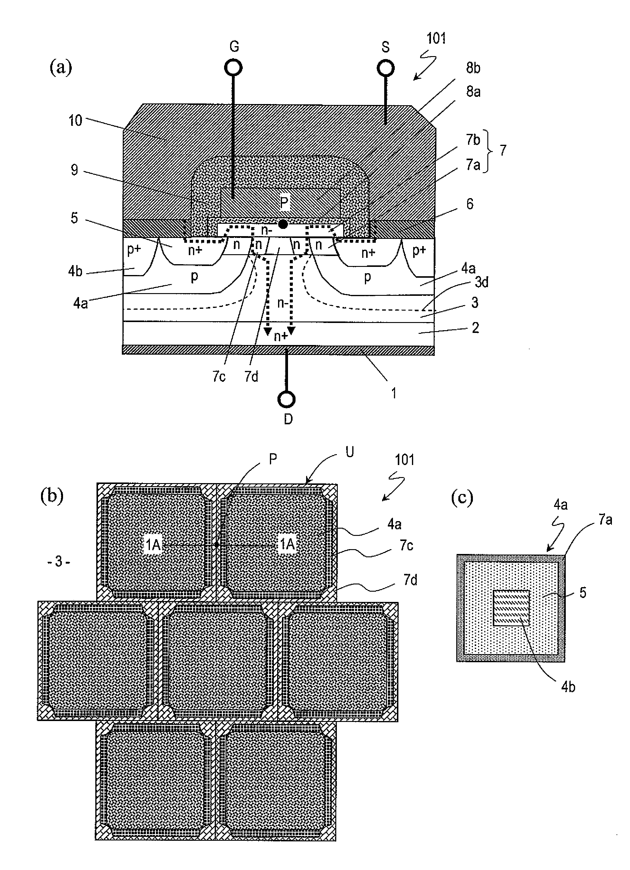
[0053]A semiconductor device according to a first embodiment of the present invention will now be described. In the present embodiment, the present invention will be described with reference to an example of a double implanted MOSFET. FIG. 1(a) shows a cross-sectional structure of a part of a double implanted MOSFET 101, and FIG. 1(b) shows a planar structure of a drift layer 3 of the MOSFET 101. FIG. 1(a) shows the cross-sectional structure taken along line 1A-1A of FIG. 1(b). The MOSFET 101 includes a plurality of unit cells U. As shown in FIG. 1(b), on the drift layer 3, each unit cell U has a rectangular shape, for example, and the unit cells U are arranged in a staggered pattern. More specifically, the unit cells U are arranged two-dimensionally, and the unit cells U are arranged with ½ period shifts in one direction. Note however that it is only required that the unit cells U are arranged at least one-dimensionally because the effects of the present invention can be obtained a...

second embodiment

[0104]A semiconductor device according to a second embodiment of the present invention will now be described. FIG. 7(a) shows a partial cross-sectional structure of a double implanted MOSFET 102, and FIG. 7(b) shows a plan view at the drift layer 3 of the MOSFET 102. FIG. 7(a) shows a cross-sectional structure taken along line 7A-7A in FIG. 7(b). In FIG. 7(b), the cross-sectional structure taken along line 1A-1A is the same as that of the first embodiment. As in the first embodiment, the MOSFET 102 includes a plurality of unit cells U, each unit cell U has a rectangular shape on the drift layer 3, and the rectangular shapes are arranged in a staggered pattern.

[0105]As shown in FIGS. 7(a) and 7(b), the MOSFET 102 is different from the first embodiment in that it further includes a fifth n-type impurity region 31 at a position in the drift layer 3 that is adjacent to the fourth n-type impurity region 7d and that includes an apex of the unit cell U. The impurity concentration of the fi...

experiment example

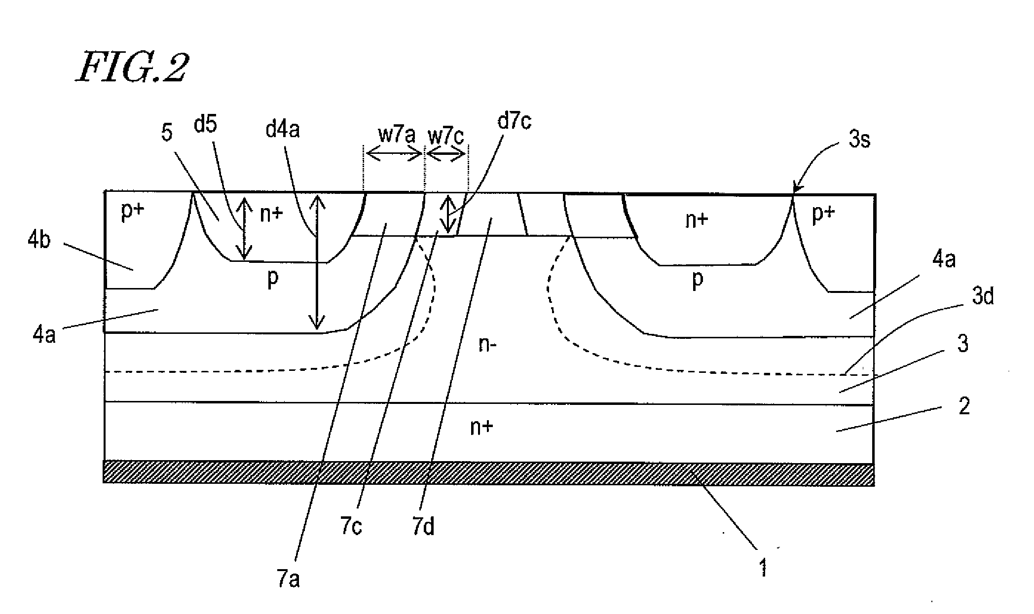
[0109]The results of an experiment on how the channel resistance is influenced when the impurity concentrations of the third n-type impurity region and the well are varied in the MOSFET 101 of the first embodiment will now be described.

[0110]As shown in FIG. 8, Xcell denotes the size of a unit cell, and a+2Lg and a respectively denote the distance between the first n-type impurity regions 5 of two adjacent unit cells and the distance between the second n-type impurity regions 7a in the direction in which the unit cells are arranged. The width of the second n-type impurity region 7a in the direction in which the unit cells are arranged is denoted as Lg which is the channel length. Table 1 shows values used in the calculation.

TABLE 1ItemSymbolUnitValueUnit cell sizeXcellμm9.6Interval between second n-type im-aμm3purity regions 7aInterval between first n-type im-a + 2Lgμm4purity regions 5Impurity concentration of well 4Nacm−3—Impurity concentration of third n-Nextcm−3—type impurity reg...


PUM


Abstract

Each unit cell includes: a drift layer 3 made of an n-type wide bandgap semiconductor formed on a substrate 2 made of an n-type wide bandgap semiconductor; a p-type well 4a provided in the driwhoseft layer 3; a first n-type impurity region 5 provided in the well 4a; a surface channel layer 7b formed at least on a surface of the well so as to connect together the first n-type impurity region 5 and the drift layer 3; a second n-type impurity region 7a provided in a surface region of the well which is under the surface channel layer and which spans the first n-type impurity region 5 and the drift layer 3, the second n-type impurity region 7a having an impurity concentration generally equal to or greater than an impurity concentration of the well 4a; and a third n-type impurity region formed in a surface region of the drift layer 3 adjacent to the second n-type impurity region 7a.

Description

TECHNICAL FIELD[0001]The present invention relates to a semiconductor device, and more particularly to a silicon carbide semiconductor device and a method for manufacturing the same.BACKGROUND ART[0002]Wide bandgap semiconductors are drawing public attention as semiconductor materials of semiconductor devices whose breakdown voltage is high and which are capable of conducting large currents therethrough (power devices). Among other wide bandgap semiconductors, silicon carbide (SiC) has a particularly high breakdown electric field, and is therefore expected as a semiconductor that is most suitable for next-generation low-loss power devices. Because good-quality silicon dioxide (SiO2) films can be formed through thermal oxidation on SiC, insulated gate-type SiC-power MOSFETs using such silicon dioxide films as gate insulating films have been developed.[0003]When an SiC-power MOSFET is manufactured, the conductivity of the semiconductor is controlled by using an ion implantation method...

Claims


Application Information

Patent Timeline
Patent Type & Authority Applications(United States)
IPC IPC(8): H01L27/088H01L21/336
CPCH01L21/047H01L29/0696H01L29/7828H01L29/4238H01L29/66068H01L29/1608
Inventor YAMASHITA, KENYA
Owner PANASONIC CORP
Why Eureka
Try Eureka