

Method and device for clock gate controlling
a clock gate and control method technology, applied in the direction of generating/distributing signals, high-level techniques, instruments, etc., can solve the problems of inconvenient use, limited to the coding style mentioned above, and the kind of coding style cannot be handled by the synthesis tools, so as to reduce the activity of large sections of the clock tree, reduce the power consumption of the circuitry system, and high coverage of the data processing block
- Summary
- Abstract
- Description
- Claims
- Application Information
AI Technical Summary
Benefits of technology
Problems solved by technology
Method used
Image

Examples
Embodiment Construction
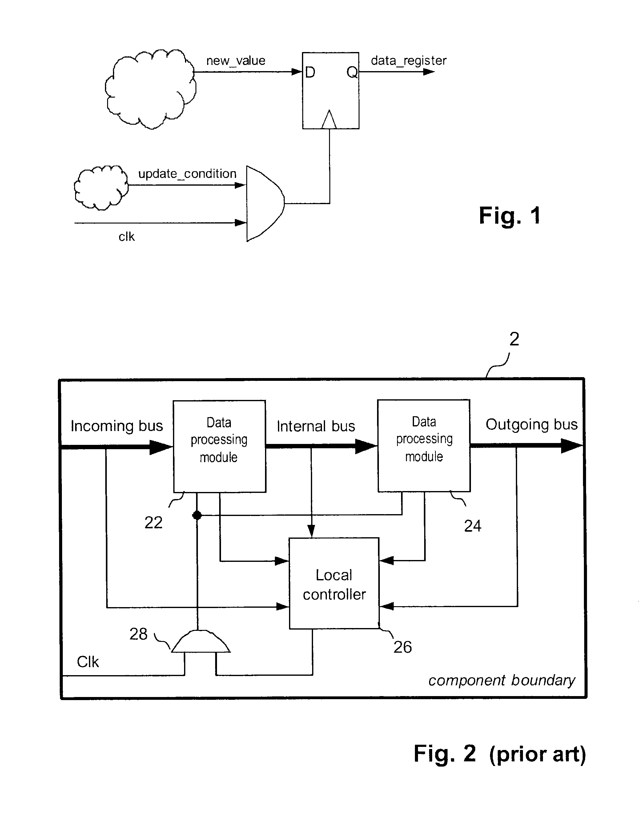
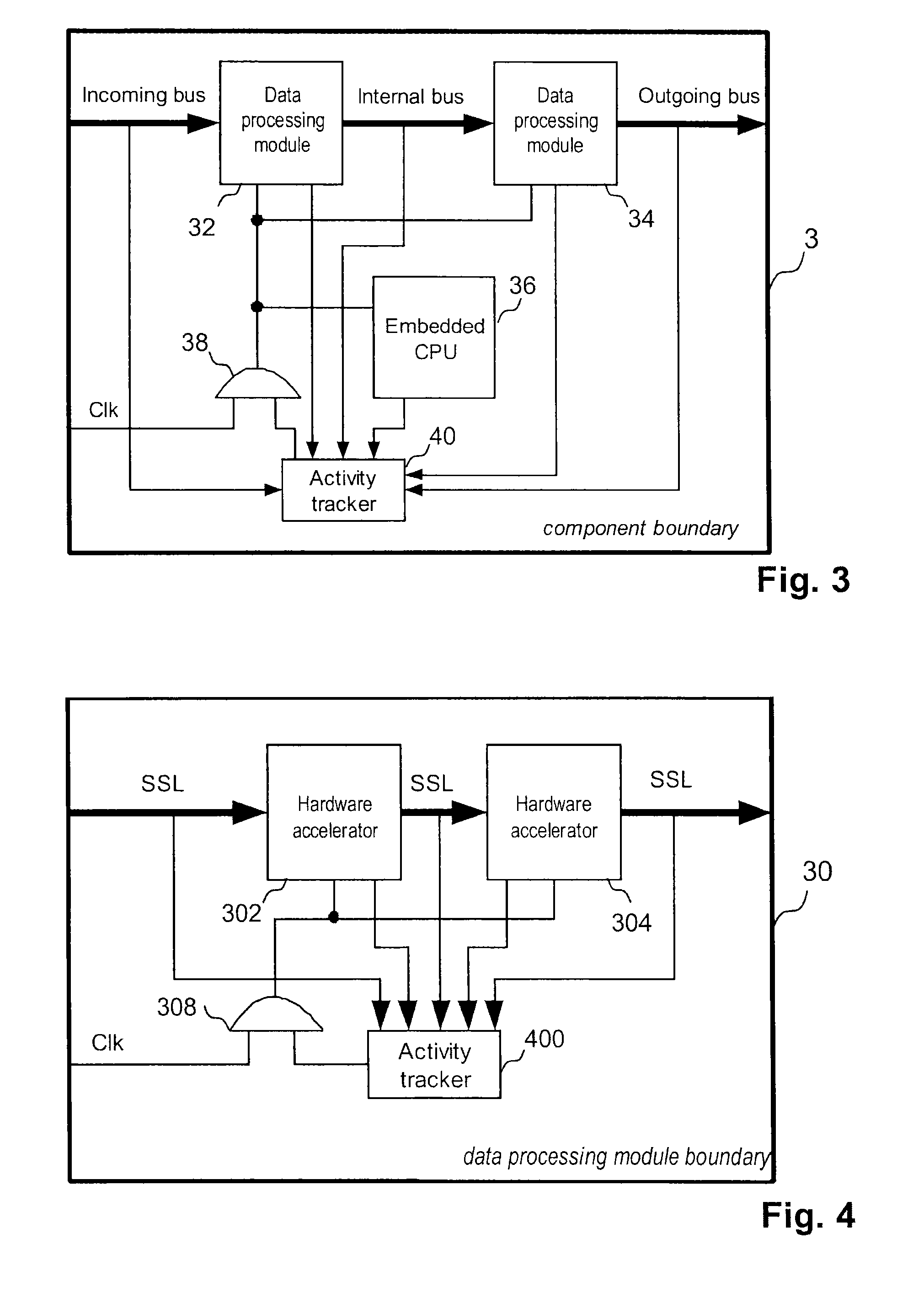
[0028]FIG. 3 shows a block diagram of a data processing component 3 which comprises data processing modules 32, 34 and an embedded controller 36. Data processing component 3 further comprises an activity tracking device 40 which receives busy indications from incoming, internal, and outgoing bus segments which are part of a streaming data bus, illustrated as bold arrows, that connect several data processing components of a circuit system such as an SoC, as well as from each of the data processing units 32, 34 connected into the streaming data bus. Activity tracker 40 may optionally receive state information from data processing units 32, 34 and from controller 36.
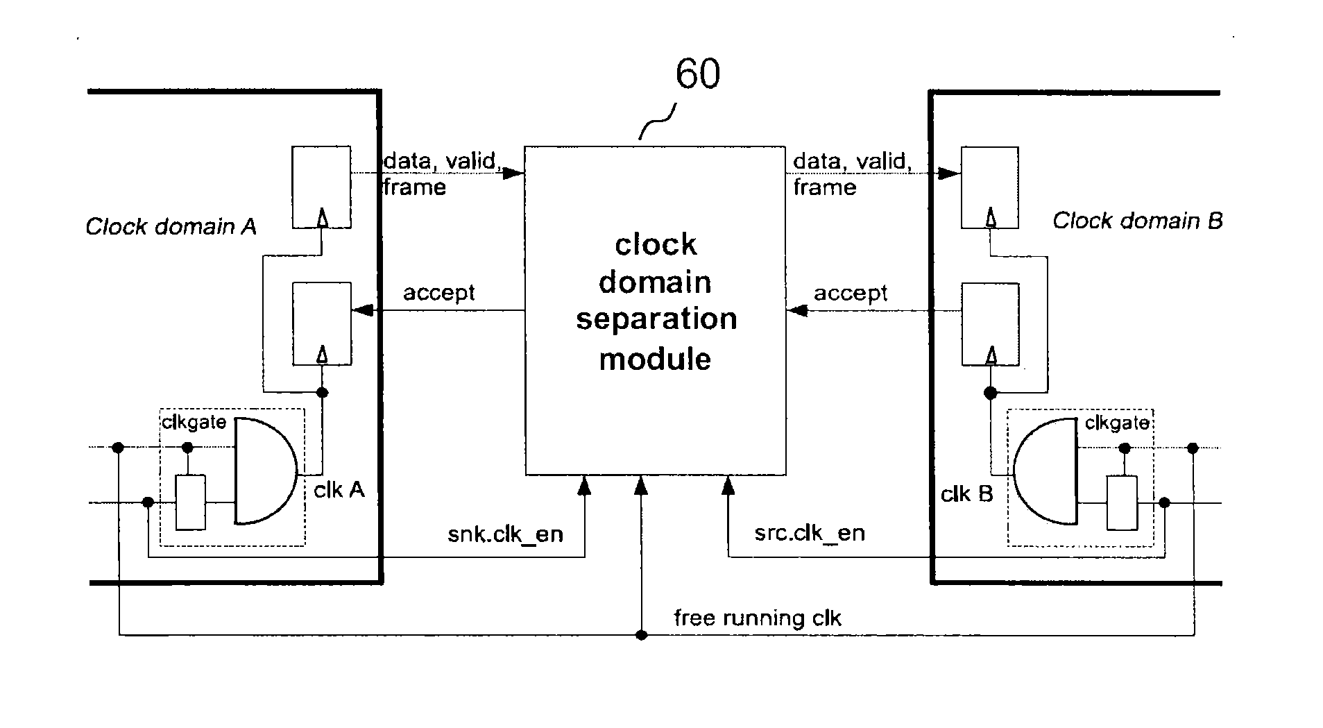
[0029]The streaming data bus uses a handshake-type transfer protocol which comprises a one-bit indication signaling the beginning and the end of a sequence of data.
[0030]FIG. 5 details the signals of a streaming data transfer protocol that can advantageously be used in one embodiment of the invention for data transfer throu...
PUM
 Abstract
Description
Claims
Application Information