Opto-electronic module with improved low power, high speed electrical signal integrity

a high-speed, electrical signal integrity technology, applied in the field of semiconductor technology, can solve the problems of low electrical signal-to-noise ratio, undesirable higher crosstalk, and difficulty in packaging the device with an electrical connector

Inactive Publication Date: 2011-08-25
GLOBALFOUNDRIES INC
View PDF34 Cites 38 Cited by
  • Summary
  • Abstract
  • Description
  • Claims
  • Application Information

AI Technical Summary

Problems solved by technology

However, the higher electrical density results in difficulty packaging the device with an electrical connector to contact an electrical flex.
However, the combination of the electrical flex with the BGA contacts results in a disadvantage of a lower electrical sign-to-noise ratio, as well as, undesirable higher crosstalk.
Further, another disadvantage of the exemplary device is that by using a four-wavelength CWDM design to reduce the

Method used


Image

  • Opto-electronic module with improved low power, high speed electrical signal integrity
  • Opto-electronic module with improved low power, high speed electrical signal integrity
  • Opto-electronic module with improved low power, high speed electrical signal integrity

Examples


Embodiment Construction

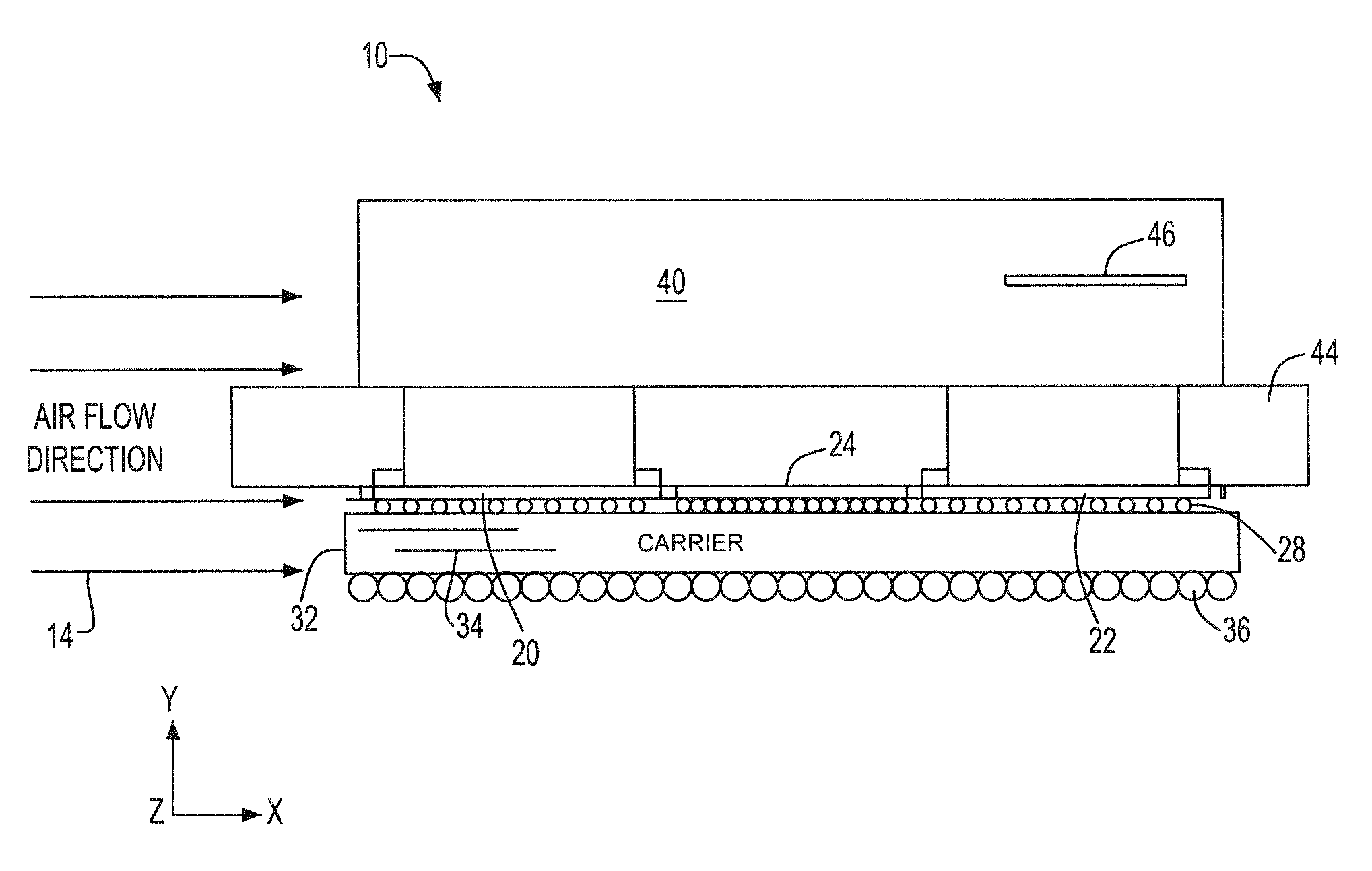
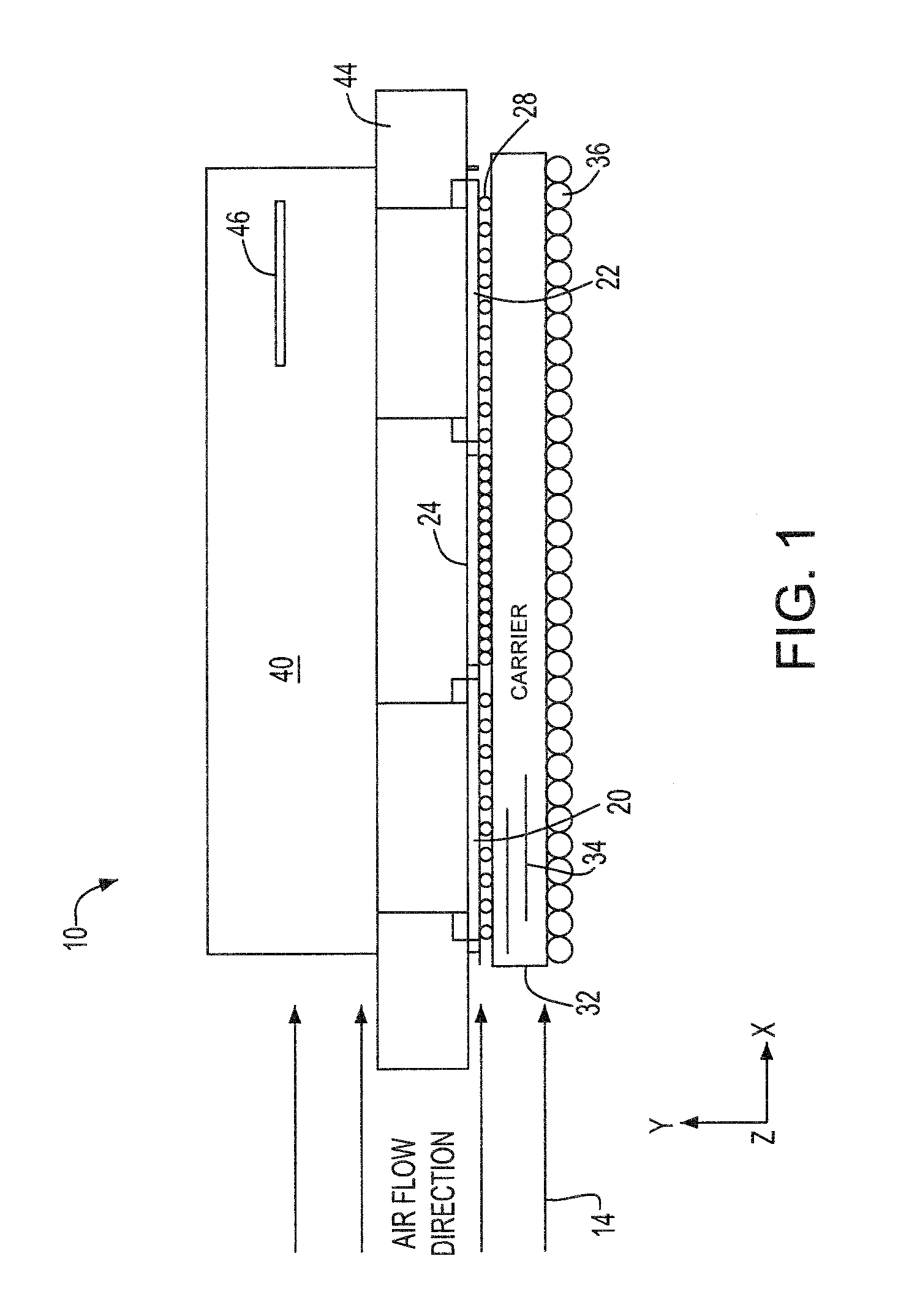
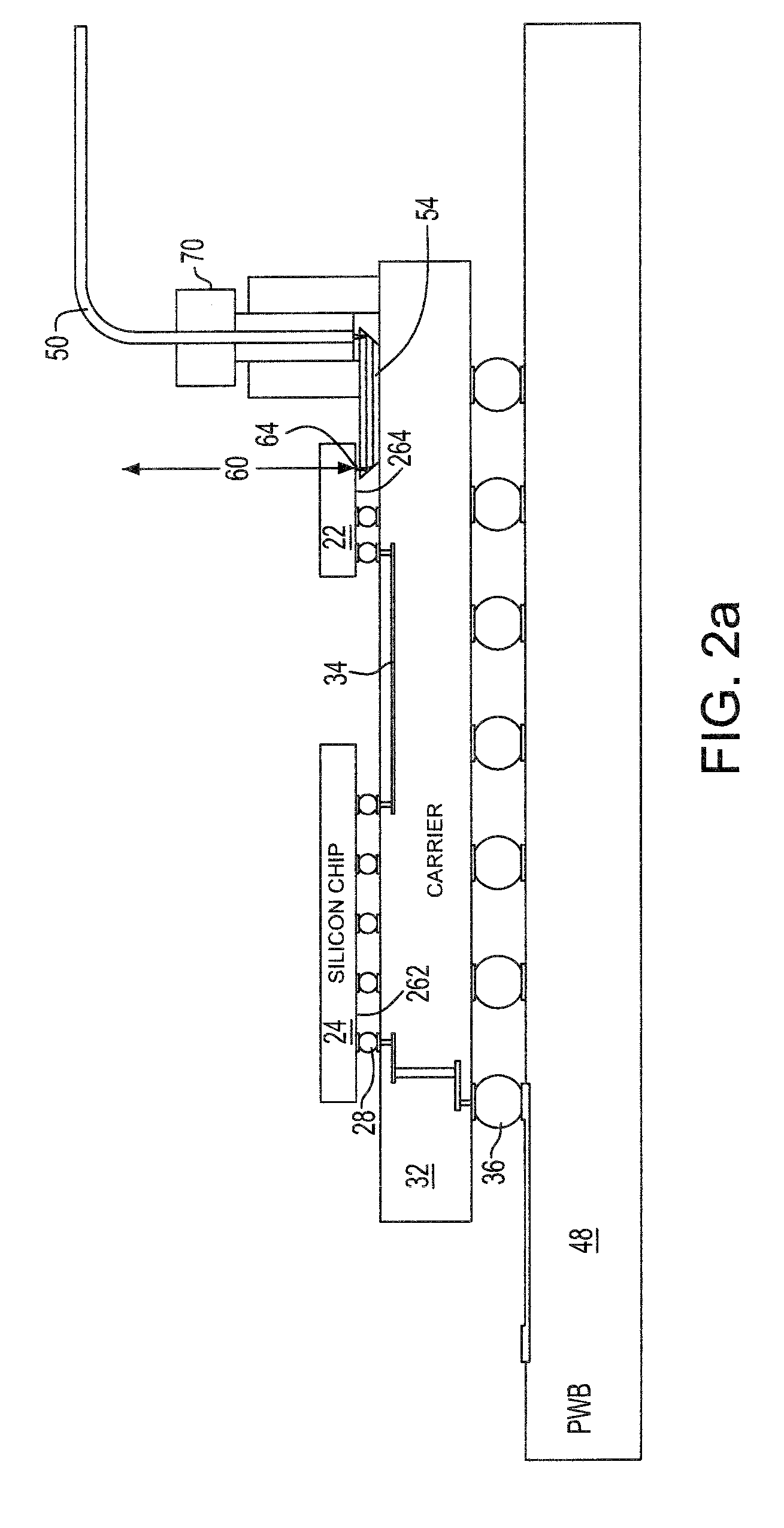
[0022]Referring to FIG. 1, in an illustrative embodiment of the present invention, a system and a method for fabrication thereof of an integrated opto-electronic (OE) package or apparatus 10 which includes one or more O / E (optical-to-electrical) modules, and / or one or more E / O modules (electrical-to-optical) 20, 22, respectively. The package 10 further includes one or more electrical chips embodied as a silicon chip 24, and an optical interface to the O / E and E / O modules 20, 22. Electrically conductive elements, in the present embodiment of the invention, C4 ball grid array (BGA) 28, is attached to the O / E and E / O modules 20, 22 and silicon chip 24, and oppositely attached to a substrate embodied as a carrier 32. The substrate may be of a material such as high performance glass ceramic, white alumina ceramic, HI-CTE (high coefficient of thermal expansion) ceramic or Flip Chip-Plastic Ball Grid Array (FC-PBGA). Also, the substrate may be comprised of multiple layers where each layer ...


PUM


Abstract

An apparatus and method for receiving electrical signals and transmitting optical signals includes a substrate having an electrical circuit. An electrical-to-optical module is mounted on the substrate, and the module includes an array of photodetectors communicating with the electrical circuit. The photodetectors may include VCSEL arrays or PD arrays. The module receives electrical signals from the electrical circuit and provides a plurality of corresponding light signals. An electrical transport is embedded in the substrate, and the electrical transport electrically communicates with the array of photodetectors. An optical interface provides electrical communication between an optical fiber and the electrical circuit. A heat transfer device may be positioned adjacent the photodetectors to transfer heat generated by the photodetectors.

Description

FIELD OF THE INVENTION[0001]The present invention generally relates to an apparatus and method for manufacturing the same in the field of semiconductor technology which provides a removable opto-electronic module and more particularly, relates to an apparatus and method in the field of integrated circuits and chip technology which provides a removable opto-electronic module.BACKGROUND[0002]In the field of semiconductor technology, one known typical device using opto-electronic modules includes a multi-channel high-density optical transmitter and receiver pair. The device reduces a fiber count by using coarse wavelength division multiplexing (CWDM). Vertical cavity surface emitting laser (VCSEL) arrays (O / E array) are used in the device and are flip-chip-attached to integrated circuits (ICs). After attachment of the O / E array to the IC, an optical coupling is added. The resulting device is compact. However, the higher electrical density results in difficulty packaging the device with...

Claims


Application Information

Patent Timeline
IPC IPC(8): H04B10/00H01L27/14G06F17/50H05K1/18
CPCH04B10/801H05K1/0203H05K1/141H05K1/181G02B6/4279H05K2201/10121G02B6/428G02B6/4214G02B6/4269H05K3/3436H01L2224/16225H01L2924/15192H01L2924/15311
Inventor BUDD, RUSSELL A.DYCKMAN, WARREN D.LAFONTANT, GARYLIBSCH, FRANK R.
Owner GLOBALFOUNDRIES INC
Why Eureka
Try Eureka