

Semiconductor device
- Summary
- Abstract
- Description
- Claims
- Application Information
AI Technical Summary
Benefits of technology
Problems solved by technology
Method used
Image

Examples
embodiment 1
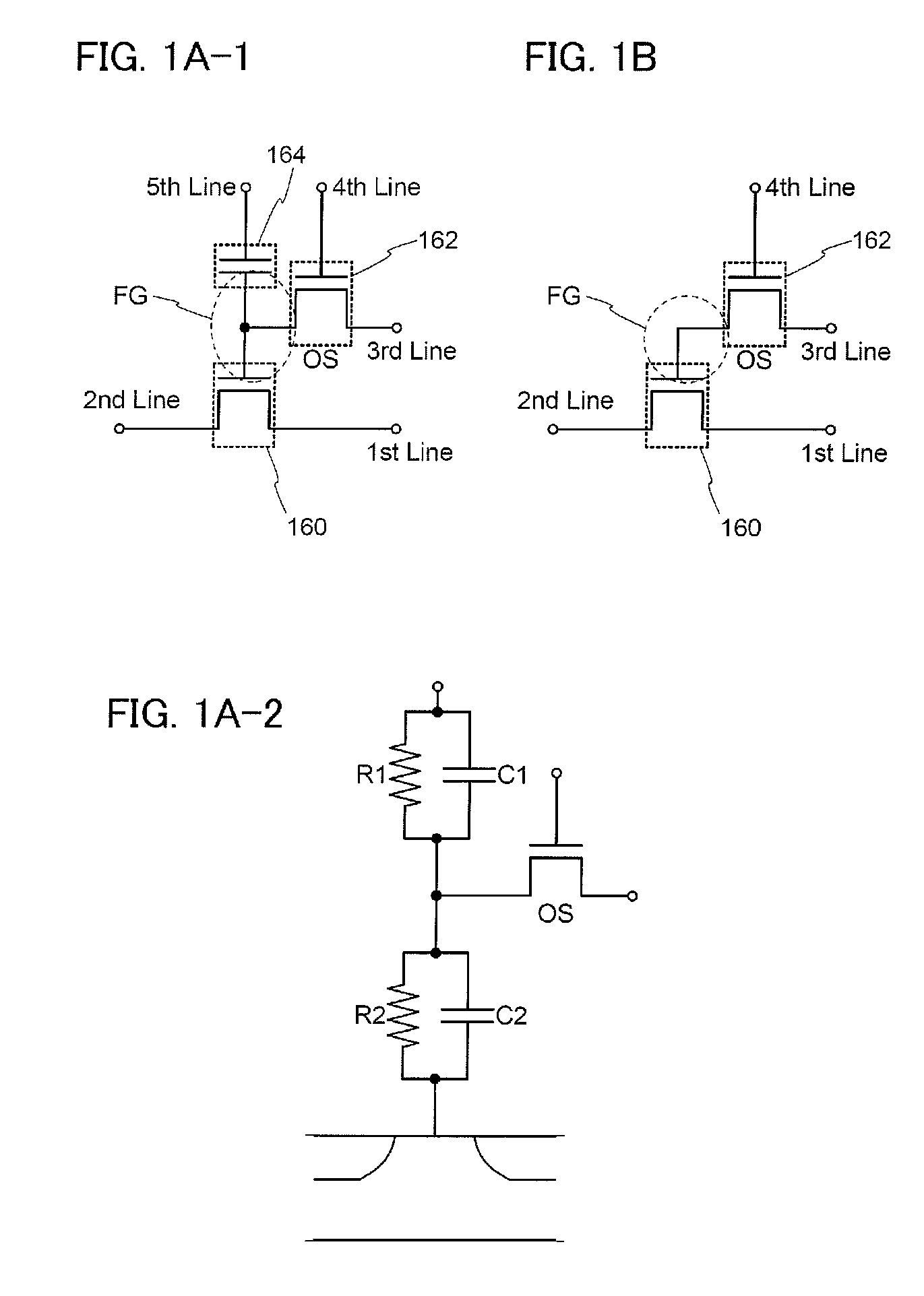
[0050]In this embodiment, a circuit configuration and operation of a semiconductor device according to an embodiment of the disclosed invention will be described with reference to FIGS. 1A-1, 1A-2, and 1B. Note that in each of circuit diagrams, in some cases, “OS” is written beside a transistor in order to indicate that the transistor includes an oxide semiconductor.
[0051]In a semiconductor device illustrated in FIG. 1A-1, a first wiring (a 1st Line, also referred to as a source line) and a source electrode of a transistor 160 are electrically connected to each other, and a second wiring (a 2nd Line, also referred to as a bit line) and a drain electrode of the transistor 160 are electrically connected to each other. In addition, a third wiring (a 3rd Line, also referred to as a first signal line) and one of a source electrode and a drain electrode of a transistor 162 are electrically connected to each other, and a fourth wiring (a 4th Line, also referred to as a second signal line) ...
embodiment 2
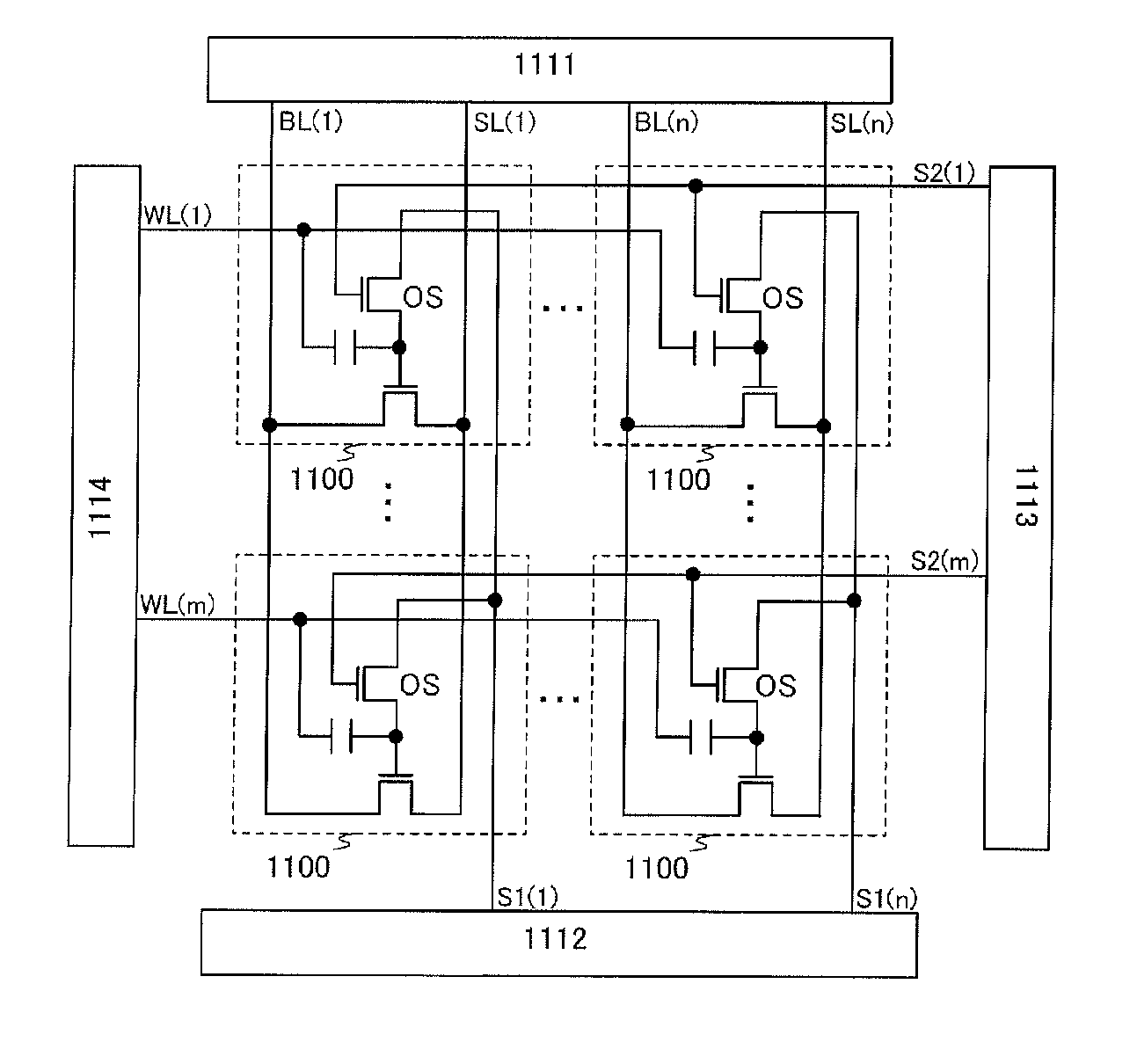
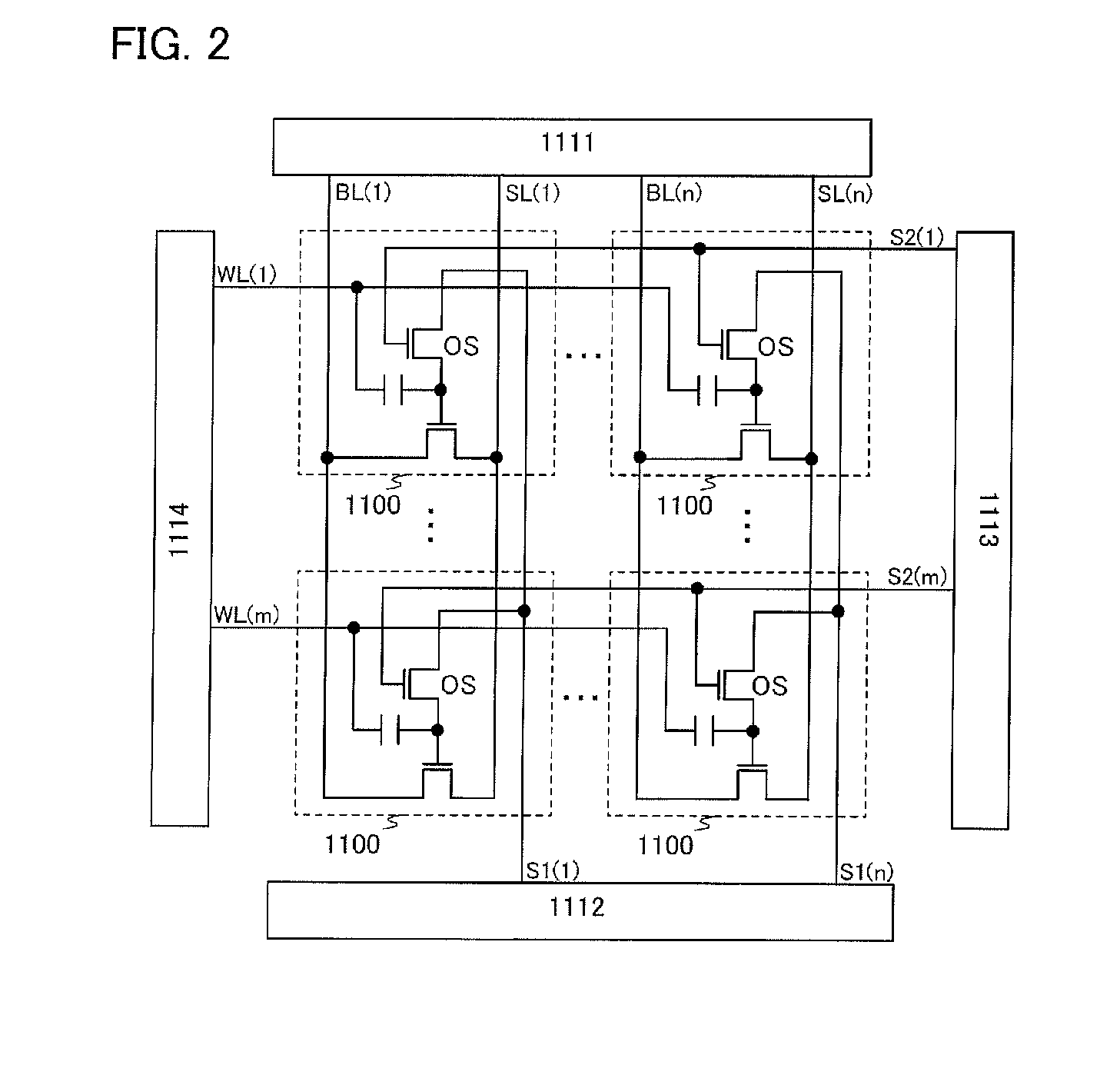
[0078]In this embodiment, an application example of the semiconductor device described in the above embodiment will be described. Specifically, an example of a semiconductor device in which the semiconductor devices described in the above embodiment are arranged in matrix will be described.
[0079]FIG. 2 is an example of a circuit diagram of a semiconductor device which has memory capacity of m×n bits.
[0080]The semiconductor device according to an embodiment of the present invention includes a memory cell array where m word lines WL (in is a natural number), in second signal lines S2, n bit lines BL (n is a natural number), n source lines SL, n first signal lines S1, and a plurality of memory cells 1100 are arranged in matrix of m (rows) (in a vertical direction)×n (columns) (in a horizontal direction) and peripheral circuits such as a first driver circuit 1111, a second driver circuit 1112, a third driver circuit 1113, and a fourth driver circuit 1114. Here, the configuration describ...
embodiment 3
[0103]In this embodiment, a structure of a semiconductor device according to an embodiment of the disclosed invention and a method for manufacturing the semiconductor device will be described with reference to FIGS. 5A and 5B, FIGS. 6A to 6D, FIGS. 7A to 7C, FIGS. 8A to 8D, and FIGS. 9A to 9C.
[0104]FIGS. 5A and 5B illustrate an example of a structure of a semiconductor device. FIG. 5A illustrates a cross section of the semiconductor device, and FIG. 5B illustrates a plan view of the semiconductor device. Here, FIG. 5A corresponds to a cross section along line A1-A2 and line B1-B2 in FIG. 5B. In the semiconductor device illustrated in FIGS. 5A and 5B, a transistor 160 including a first semiconductor material is included in a lower portion, and a transistor 162 including a second semiconductor material is included in an upper portion. Here, it is preferable that the first semiconductor material and the second semiconductor material be different materials. For example, the first semico...
PUM
 Abstract
Description
Claims
Application Information