

Power conversion apparatus and control method for power conversion apparatus
- Summary
- Abstract
- Description
- Claims
- Application Information
AI Technical Summary
Benefits of technology
Problems solved by technology
Method used
Image


Examples
embodiment 1
Modification of Embodiment 1
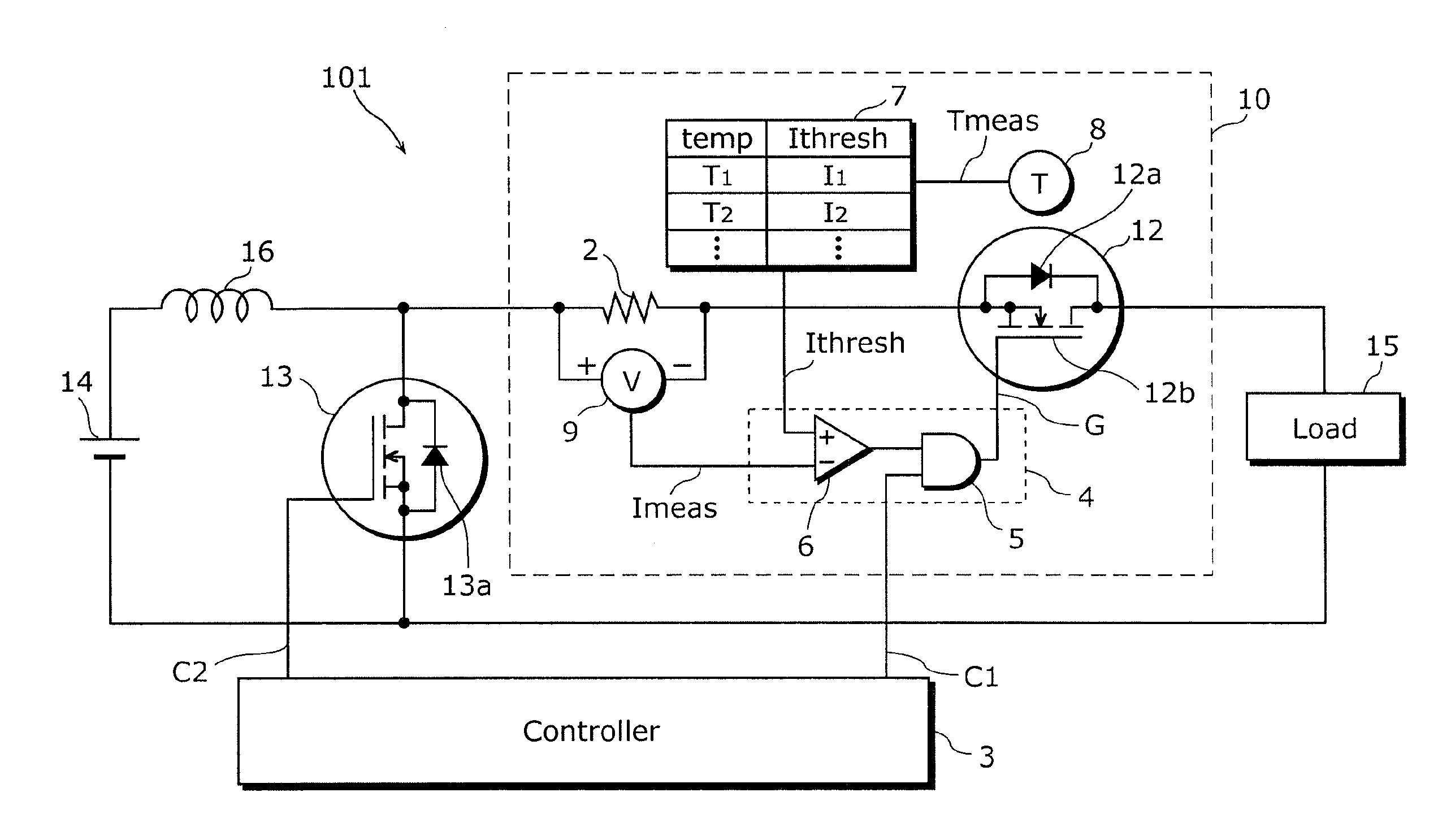
[0124]Described next is a buck converter exemplified as the power conversion apparatus in accordance with the present invention.
[0125]FIG. 5 is a circuit diagram exemplifying a conventional buck converter.
[0126]A buck converter 200 shown in FIG. 5 is the boost converter 100 shown in FIG. 11 with the power source 14 and the load 15 replaced.
[0127]The buck converter serving as a power conversion apparatus in accordance with the present invention is built with the MOSFET 12, included in the buck converter 200, replaced with the synchronous rectifying circuit 10 described in Embodiment 1.
[0128]FIG. 6 is a functional block diagram exemplifying a structure of a buck converter 201 serving as a power conversion apparatus in accordance with Embodiment 1 of the present invention.
[0129]In the buck converter 201, the synchronous rectifying circuit 10 operates in a same manner as so in the boost converter 101. Thus, the synchronous rectifying circuit 10 can autonomous...
embodiment 2
[0133]Described as Embodiment 2 is a modification of a synchronous rectification circuit including MOSFETs.
[0134]FIG. 7 is a functional block diagram exemplifying a structure of a synchronous rectifying circuit 22 in accordance with Embodiment 2 of the present invention. The synchronous rectification circuit 22 is different from the synchronous rectifying circuit 10 shown in FIG. 1 in having (i) the MOSFETs 12 connected in parallel and commonly controlled via the gate signal “G”, and (ii) the shunt resistor 2 connected in series only to a single representative MOSFET (the MOSFET 12 placed on the top in FIG. 7) among the MOSFETs 12.
[0135]Having the MOSFETs 12 connected in parallel, the synchronous rectification circuit 22 is suitable for handling a large amount of current. The MOSFETs 12 and the shunt resistor 2 included in the synchronous rectification circuit 22 may be contained in one package and formed into an IPM 11.
[0136]The synchronous rectification circuit 22 structured above...
embodiment 3
[0138]Described next are a full bridge inverter and a three-phase inverter exemplified as a power conversion apparatus in accordance with the present invention.
[0139]FIG. 8A is a functional block diagram exemplifying a structure of a full bridge inverter 301 serving as a power conversion apparatus in accordance with Embodiment 3 of the present invention.
[0140]The full bridge inverter 301 has four switching elements replaced with respective four synchronous rectifying circuits 10, including the synchronous rectifying circuit 10 described above. Such switching elements are included in a bridge circuit of a typical full bridge inverter. Each of the synchronous rectifying circuits 10 is referred to as synchronous rectifying circuits 10a to 10d to be distinguished each other. The full bridge inverter 301 includes an inductor 17 and a capacitor 18 both used for smoothing.
[0141]The pairs of the synchronous rectifying circuits 10a and 10d, and the synchronous rectifying circuits 10b and 10c...
PUM
 Abstract
Description
Claims
Application Information