Nitrogen doped amorphous carbon hardmask

a carbon hardmask and nitrogen doping technology, applied in the direction of chemical vapor deposition coating, coating, plasma technique, etc., can solve the problems of low-k dielectric material devices with little or no surface defects or feature deformation, and increase the likelihood of defects on the substrate surfa

Inactive Publication Date: 2011-10-06
APPLIED MATERIALS INC
View PDF2 Cites 68 Cited by
  • Summary
  • Abstract
  • Description
  • Claims
  • Application Information

AI Technical Summary

Benefits of technology

[0010]Embodiments of the present invention generally relate to the fabrication of integrated circuits and more particularly to nitrogen doped amorphous carbon layers and processes for depositing nitrogen doped amorphous carbon layers on a semiconductor substrate. In one embodiment, a method of forming a nitrogen doped amorphous carbon layer on a substrate is provided. The method comprises positioning a substrate in a substrate processing chamber, introducing a nitrogen containing hydrocarbon source into the processing chamber, introducing a hydrocarbon source into the processing chamber, introducing a plasma-initiating gas into the processing chamber, generating a plasma in the processing chamber, and forming a nitrogen doped amorphous carbon layer on the substrate.
[0011]In another embodiment, a method of forming a device is provided. the method comprises forming one or more nitrogen doped amorphous carbon layers on a substrate by positioning a substrate in a deposition chamber, providing a gas mixture to the deposition chamber, wherein the gas mixture comprises a nitrogen containing hydrocarbon source, one or more hydrocarbon compounds and an inert gas, and generating a plasma in the processing chamber to decompose the one or more hydrocarbon compounds and the nitrogen containing hydrocarbon source in the gas mixture to form the one or more nitrogen doped amorphous carbon layers on the substrate, defining a pattern in at least one region of the one or more nitrogen doped amorphous carbon layers, and transferring the pattern defined in the at least one region of the one or more nitrogen doped amorphous carbon layers into the substrate using the one or more nitrogen doped amorphous carbon layers as a mask.

Problems solved by technology

Integrated circuits have evolved into complex devices that can include millions of transistors, capacitors and resistors on a single chip.
Producing devices having low-k dielectric materials with little or no surface defects or feature deformation is problematic.
Low-k dielectric materials having a dielectric constant less than about 3.0 are often porous and susceptible to being scratched or damaged during subsequent process steps, thus increasing the likelihood of defects being formed on the substrate surface.
Such low-k dielectric materials are often brittle and may deform under conventional polishing processes, such as chemical mechanical polishing (CMP).
As device sizes shrink and pattern structure becomes more complex and difficult to manufacture, an etch hardmask is becoming more important as available photoresists are failing to meet the etching resistance requirements and photoresists are simply being used for image transfer rather than as an etch mask in a lithography and etching process.
The former option increases the number of production steps, resulting in higher cost per wafer as well as complex integration issues.

Method used


Image

  • Nitrogen doped amorphous carbon hardmask
  • Nitrogen doped amorphous carbon hardmask
  • Nitrogen doped amorphous carbon hardmask

Examples


example 1

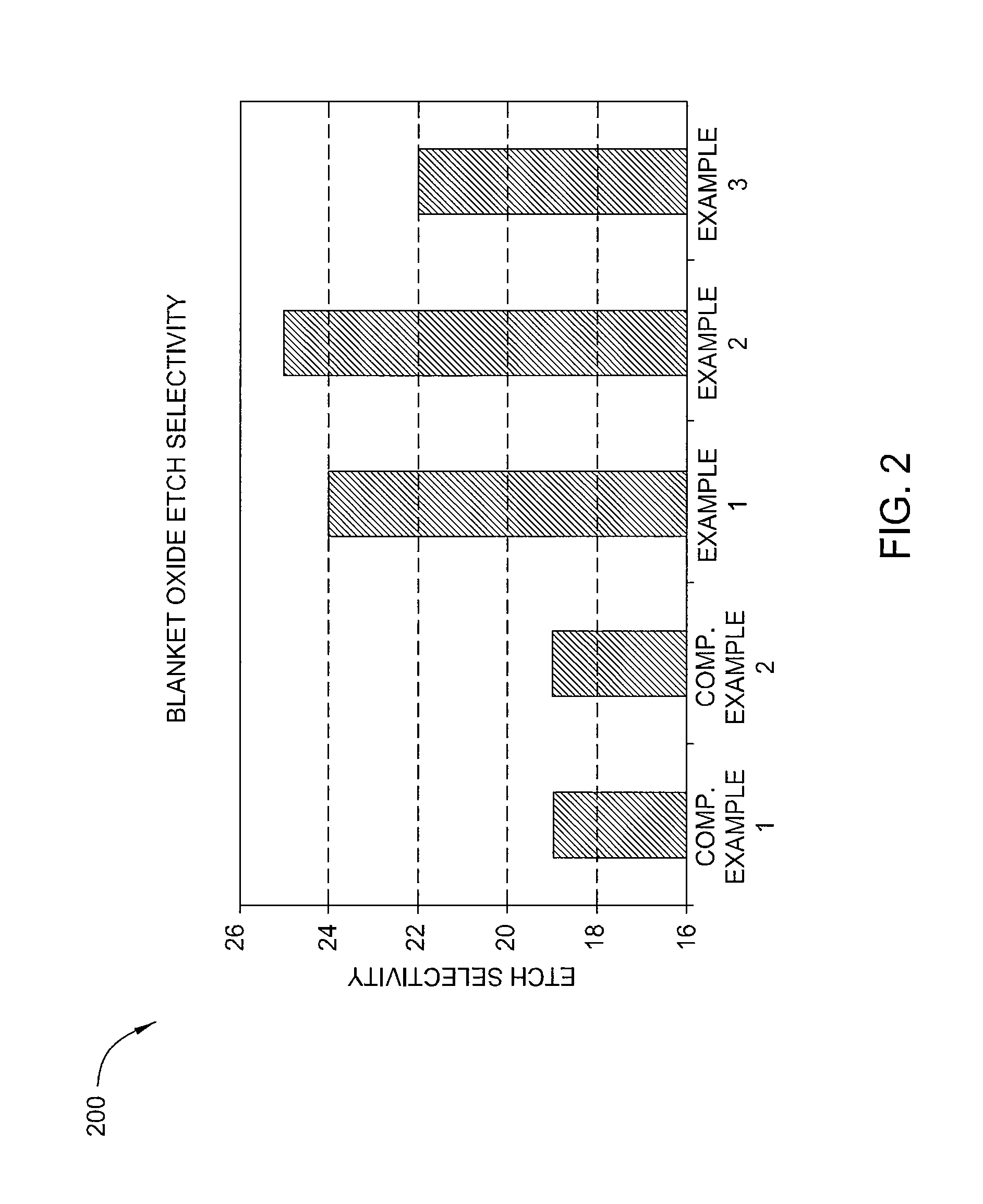
[0051]A nitrogen doped amorphous carbon deposition process example includes providing a flow rate of helium to the processing chamber at about 400 sccm, a flow rate of Argon to the processing chamber at about 14,000 sccm, providing a flow rate of C2H2 to the processing chamber at about 600 sccm, and providing a flow rate of trimethylamine to the processing chamber at about 200 sccm, applying a high frequency RF power (13.56 MHz) at about 1,400 W, maintaining a deposition temperature of about 400° C., maintaining a chamber pressure of about 3.5 Torr, with a spacing of about 300 mils to produce a nitrogen doped amorphous carbon layer having an etch selectivity of about 24.

example 2

[0052]A nitrogen doped amorphous carbon deposition process example includes providing a flow rate of helium to the processing chamber at about 400 sccm, a flow rate of Argon to the processing chamber at about 14,000 sccm, providing a flow rate of C2H2 to the processing chamber at about 600 sccm, and providing a flow rate of trimethylamine to the processing chamber at about 500 sccm, applying a high frequency RF power (13.56 MHz) at about 1,400 W, maintaining a deposition temperature of about 400° C., maintaining a chamber pressure of about 3.5 Torr, with a spacing of about 300 mils to produce a nitrogen doped amorphous carbon layer having an etch selectivity of about 25.

example 3

[0053]A nitrogen doped amorphous carbon deposition process example includes providing a flow rate of helium to the processing chamber at about 400 sccm, a flow rate of Argon to the processing chamber at about 14,000 sccm, providing a flow rate of C2H2 to the processing chamber at about 600 sccm, and providing a flow rate of trimethylamine to the processing chamber at about 1,000 sccm, applying a high frequency RF power (13.56 MHz) at about 1,400 W, maintaining a deposition temperature of about 400° C., maintaining a chamber pressure of about 3.5 Torr, with a spacing of about 300 mils to produce a nitrogen doped amorphous carbon layer having an etch selectivity of about 22.

[0054]The Blanket Oxide Etch Selectivity results for comparative examples 1 and 2 and examples 1, 2, and 3 are depicted in FIG. 2. FIG. 2 is a plot 200 depicting the blanket oxide etch selectivity of nitrogen doped amorphous carbon layers formed with varying levels of nitrogen dopant in comparison with previously k...


PUM

PropertyMeasurementUnit
pressureaaaaaaaaaa
densityaaaaaaaaaa
temperatureaaaaaaaaaa

Abstract

Embodiments described herein generally relate to the fabrication of integrated circuits and more particularly to nitrogen doped amorphous carbon layers and processes for depositing nitrogen doped amorphous carbon layers on a semiconductor substrate. In one embodiment, a method of forming a nitrogen doped amorphous carbon layer on a substrate is provided. The method comprises positioning a substrate in a substrate processing chamber, introducing a nitrogen containing hydrocarbon source into the processing chamber, introducing a hydrocarbon source into the processing chamber, introducing a plasma-initiating gas into the processing chamber, generating a plasma in the processing chamber, and forming a nitrogen doped amorphous carbon layer on the substrate.

Description

BACKGROUND OF THE INVENTION[0001]1. Field of the Invention[0002]Embodiments of the present invention generally relate to the fabrication of integrated circuits and more particularly to nitrogen doped amorphous carbon layers and processes for depositing nitrogen doped amorphous carbon layers on a semiconductor substrate.[0003]2. Description of the Related Art[0004]Integrated circuits have evolved into complex devices that can include millions of transistors, capacitors and resistors on a single chip. The evolution of chip design continually requires faster circuitry and greater circuit density. The demand for faster circuits with greater circuit densities imposes corresponding demands on the materials used to fabricate such integrated circuits. In particular, as the dimensions of integrated circuit components are reduced to sub-micron dimensions, it has been necessary to use not only low resistivity conductive materials such as copper to improve the electrical performance of devices,...

Claims


Application Information

Patent Timeline
Patent Type & Authority Applications(United States)
IPC IPC(8): C23C16/513
CPCC23C16/26H01L21/02118H01L21/3065H01L21/0273H01L21/02274H01L21/02592
Inventor CHENG, SIU F.JANZEN, JACOBPADHI, DEENESHKIM, BOK HOEN
Owner APPLIED MATERIALS INC
Why Eureka
Try Eureka