Chemical Bath Deposition Apparatus for Fabrication of Semiconductor Films through Roll-to-Roll Processes

Inactive Publication Date: 2011-10-20
WANG JIAXIONG
View PDF1 Cites 31 Cited by
  • Summary
  • Abstract
  • Description
  • Claims
  • Application Information

AI Technical Summary

Benefits of technology

[0012]The present invention provides a roll-to-roll or reel-to-reel chemical bath deposition apparatus and the related method to fabricate semiconductor thin films in preparation of solar cells. It possesses a unique design to vertically deliver a flexible foil through the whole apparatus. The deposition solution is continuously sprayed onto the substrate surface through a whole process from a freshly mixed to an aged stage. During the whole process, the backside of a substrate remains dry. The structure of this equipment is very simple and inexpensive. In addition, the preparation of semicon

Problems solved by technology

Moreover, the potential radiation contamination arising from the nuclear energy may bring serious problems to our environment, especially after the recent accident in a nuclear power station of Japan.
Besides, it has a problem of power degradation with initial illumination, but its technology is relatively mature.
However, a superstrate configuration may not be applicable on a flexible workpiece on the basis of current technology.
The disadvantage is that it produces lots of cadmium wastes and the post-treatment may be a heavy work.
However, Cd(OH)2 will dissolve in the ammonia alkaline solution to become [Cd(NH3)4]2+ complex cations and not affect the quality of the CdS product.
The reaction starting from

Method used


Image

  • Chemical Bath Deposition Apparatus for Fabrication of Semiconductor Films through Roll-to-Roll Processes
  • Chemical Bath Deposition Apparatus for Fabrication of Semiconductor Films through Roll-to-Roll Processes
  • Chemical Bath Deposition Apparatus for Fabrication of Semiconductor Films through Roll-to-Roll Processes

Examples


example

A CdS Film Deposition for Fabrication of a CIGS Solar Cell

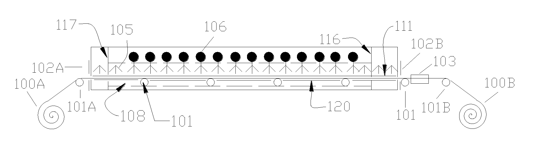
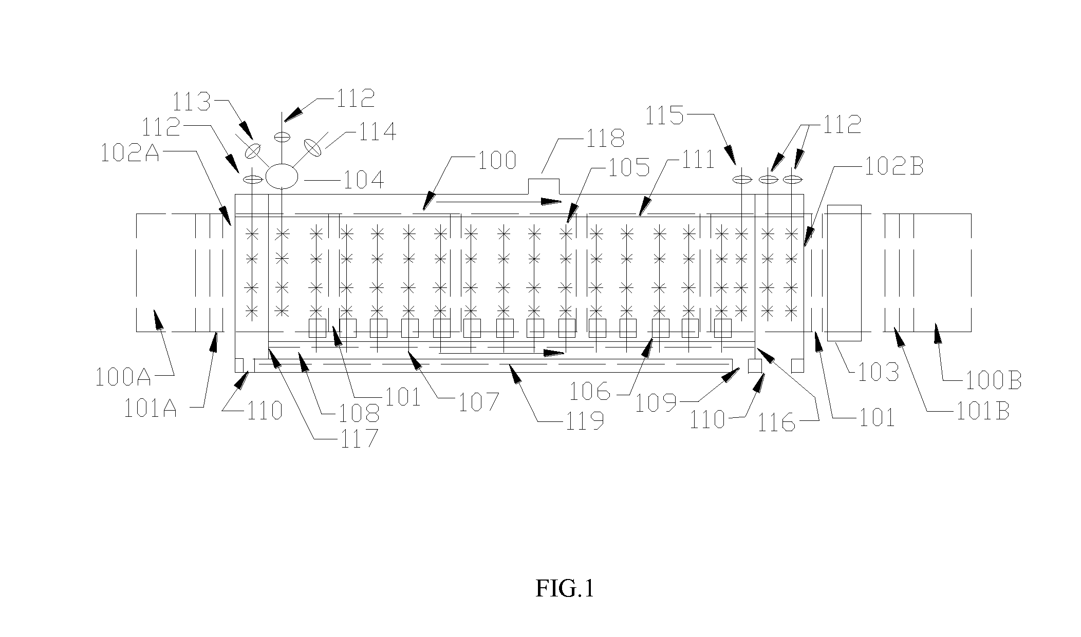
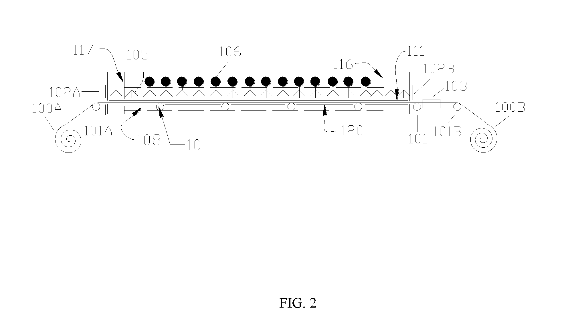
[0027]The present invention can be demonstrated with an example to deposit a CdS thin film on the surface of a CIGS absorber layer, as shown in FIG. 4. This figure is a schematic diagram illustrating the deposition of a CdS buffer 404 onto a CIGS absorber layer 403 that is coated on a piece of stainless steel substrate 401 isolated with a Mo layer 402. As an example, a 1000 meter long and 1 meter wide stainless steel roll coated with CIGS absorber layer may be used and delivered at a speed of 1 meter per minute. The main reaction chamber between the separation boards 117 and 116 is designed to be 12 meters long to meet a 12 minutes of reaction time. If the CIGS surface is assumed to be covered with a 3 mm thick solution during the deposition, 3 liters of solution shall be consumed in one minute and totally 3 m3 of solution has to be used for the whole roll. To increase the efficiency of the spray, one may want to increase the...


PUM

PropertyMeasurementUnit
Thicknessaaaaaaaaaa
Lengthaaaaaaaaaa
Volumeaaaaaaaaaa

Abstract

A chemical bath deposition method and a system are presented to prepare different thin films on continuous flexible substrates in roll-to-roll processes. In particular, they are useful to deposit CdS or ZnS buffer layers in manufacture of thin film solar cells. This method and the deposition system deposit thin films onto vertically travelling continuous flexible workpieces delivered by a roll-to-roll system. The thin films are deposited with continuously spraying the reaction solutions from their freshly mixed styles to gradually aged forms until the designed thickness is obtained. The substrates and the solutions are heated to a reaction temperature. During the deposition processes, the front surfaces of the flexible substrates are totally covered with the sprayed solutions but the substrate backsides are remained dry. The reaction ambience inside the reactor can be isolated from the outside atmosphere. The apparatus is designed to generate a minimum amount of waste solutions for chemical treatments.

Description

FIELD OF THE INVENTION[0001]The present invention relates to a chemical bath deposition (CBD) apparatus and a method that can be used to deposit semiconductor thin films onto flexible substrates continuously delivered through a roll-to-roll or reel-to-reel process. It is particularly useful for deposition of cadmium sulfide (CdS) or zinc sulfide (ZnS) semiconductor films for fabrication of thin film solar cells.BACKGROUND[0002]Photovoltaic technology has been developed under a background of global warming and exhausting of fossil fuels. The substitutes of traditional energy sources include nuclear energy and renewable energy. Among them, the nuclear energy will also be exhausted in the future. Moreover, the potential radiation contamination arising from the nuclear energy may bring serious problems to our environment, especially after the recent accident in a nuclear power station of Japan. Therefore, our future may greatly rely on renewable energy. The photovoltaic devices, or sola...

Claims


Application Information

Patent Timeline
IPC IPC(8): H01L31/18B05C11/00B05C1/00B05C13/02
CPCH01L31/18C23C18/08C23C18/1204H01L31/0296Y02E10/541H01L31/206C23C18/1208C23C18/1291H01L31/0322C23C18/12C23C18/1216Y02P70/50
Inventor WANG, JIAXIONG
Owner WANG JIAXIONG
Why Eureka
Try Eureka