Systems and methods for growing monocrystalline silicon ingots by directional solidification

a monocrystalline silicon and ingot technology, applied in the direction of crystal growth process, polycrystalline material growth, chemistry apparatus and processes, etc., can solve the problems of reducing the efficiency of any device formed, so as to achieve high quality, time saving, and retain cost efficiency

Inactive Publication Date: 2011-10-27
GT SOLAR INC
View PDF4 Cites 21 Cited by
  • Summary
  • Abstract
  • Description
  • Claims
  • Application Information

AI Technical Summary

Benefits of technology

The subject invention relates to systems and methods for producing materials, such as silicon, having a monocrystalline structure. The subject invention can achieve the benefit of producing a high quality monocrystalline product while retaining the cost efficiency and time savings achieved by known directional solidification techniques.
In operation, a gas introduced into the heat exchanger can be controlled by feedback obtained by monitoring melting of the feedstock material and the seed crystal or from the thermocouple positioned inside the heat exchanger near the bottom of the crucible. In response to the feedback, a gas flow into the heat exchanger is increased, thus increasing heat extraction by the heat exchanger, to promote directional solidification off the seed crystal.

Problems solved by technology

Since defects in conventional crystal structures typically occur at the grain boundaries, these defects tend to degrade the electrical and thermal properties of the material.
The numerous defects at the grain boundaries of a multicrystalline structure can reduce the efficiency of any device which is formed relative to a device formed from a monocrystalline material.
The Czochralski method, while it produces nearly defect free silicon ingots, is very expensive.
Another disadvantage is the increased impurity content (such as oxygen) introduced by the crucible.
During pulling of the ingot, these secondary phases can result in structural breakdown, resulting in a lower quality product.
Because of the added cost of the Czochralski process, crystalline silicon wafers produced for photovoltaic applications generally are multicrystalline.
As mentioned above, defects typically occur with multicrystalline structures, and can result in non-uniform properties in the silicon ingot.

Method used


Image

  • Systems and methods for growing monocrystalline silicon ingots by directional solidification
  • Systems and methods for growing monocrystalline silicon ingots by directional solidification
  • Systems and methods for growing monocrystalline silicon ingots by directional solidification

Examples


Embodiment Construction

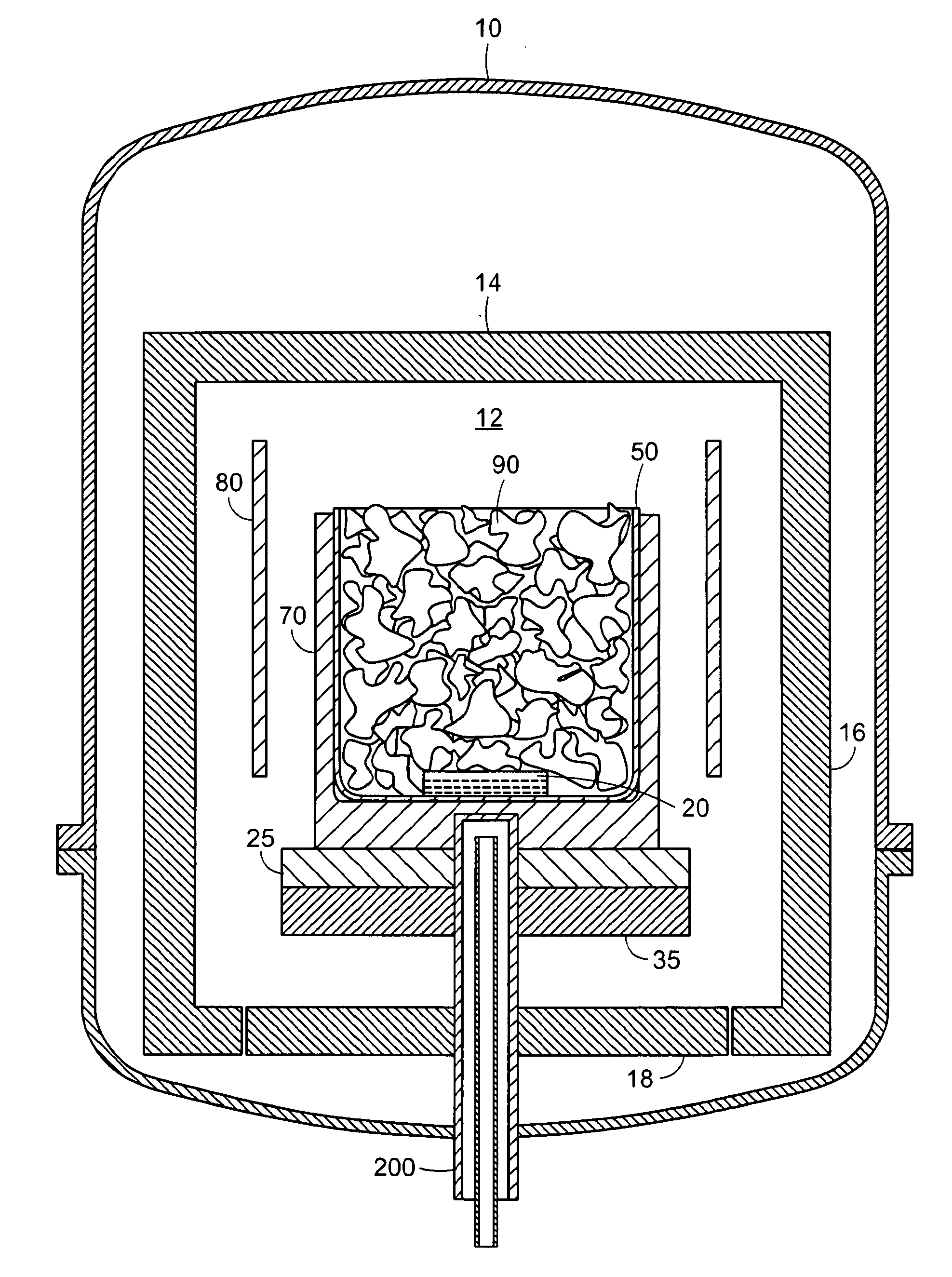
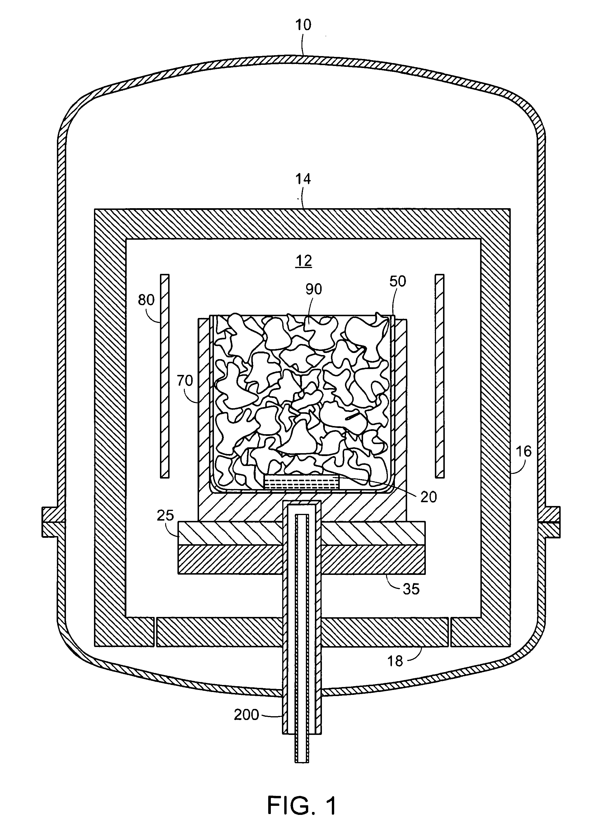
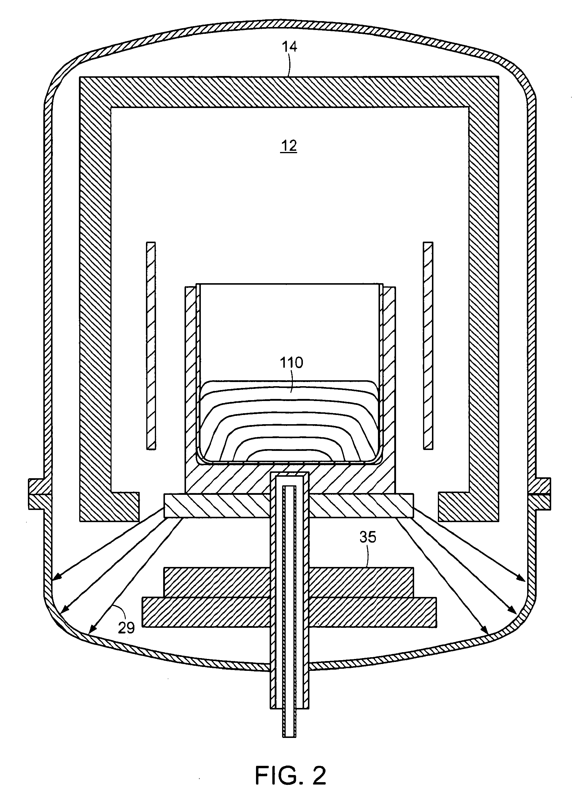
Preferred embodiments of the subject invention are described below with reference to the accompanying drawings, in which like reference numerals represent the same or similar elements.

The subject invention relates to systems and methods of growing monocrystalline materials. While the description herein discusses production of monocrystalline silicon, the techniques and methods described herein are not limited to the production of monocrystalline silicon or silicon only. A number of monocrystalline materials can be produced using the method of the subject invention such as semiconductor crystals (for example, Ge, GaAs, etc.), oxides (for example, sapphire, YAG, ALON), and fluorides (for example, MgF2, CaF2), etc.

Current efforts to commercially produce monocrystalline materials such as silicon generally employ radiant heat extraction. The system and method of the subject invention can be used to produce monocrystalline ingots by modifying the directional solidification process to prod...


PUM

PropertyMeasurementUnit
diameteraaaaaaaaaa
diameteraaaaaaaaaa
pressureaaaaaaaaaa

Abstract

Systems and methods are provided for producing monocrystalline materials such as silicon, the monocrystalline materials being usable in semiconductor and photovoltaic applications. A crucible (50) is received in a furnace (10) for growing a monocrystalline ingot, the crucible (50) initially containing a single seed crystal (20) and feedstock material (90), where the seed crystal (20) is at least partially melted, and the feedstock material (90) is completely melted in the crucible (50), which is followed by a growth and solidification process. Growth of monocrystalline materials such as silicon ingots is achieved by directional solidification, in which heat extraction during growth phases is achieved using insulation (14) that is movable relative to a crucible (50) containing feedstock (90). A heat exchanger (200) also is provided to control heat extraction from the crucible (50) during the growth and solidification process to achieve monocrystalline growth.

Description

FIELD OF INVENTIONThe subject invention is directed to systems and methods for producing monocrystalline materials. More particularly, the subject invention relates to systems and methods for producing monocrystalline silicon for solar cell applications.DESCRIPTION OF THE RELATED ARTA monocrystalline structure can be exhibited by a solid material in which the crystal lattice of the entire structure is continuous and unbroken to the edges of the structure, with substantially low defects and no grain boundaries. Since defects in conventional crystal structures typically occur at the grain boundaries, these defects tend to degrade the electrical and thermal properties of the material. As a result, high interfacial energy and relatively weak bonding in most grain boundaries can make them preferred sites for the onset of problems and for the precipitation of new unwanted phases of the solid. A multicrystalline structure generally is a crystalline material that is produced in such a way t...

Claims


Application Information

Patent Timeline
Patent Type & Authority Applications(United States)
IPC IPC(8): C30B11/02
CPCC30B11/003C30B11/007Y10T117/1004Y10T117/1092C30B29/06Y02E10/50C30B11/00H01L31/04
Inventor KHATTAK, CHANDRA P.PARTHASARATHY, SANTHANA RAGHAVANRAVI, BHUVARAGASAMY G.
Owner GT SOLAR INC
Why Eureka
Try Eureka