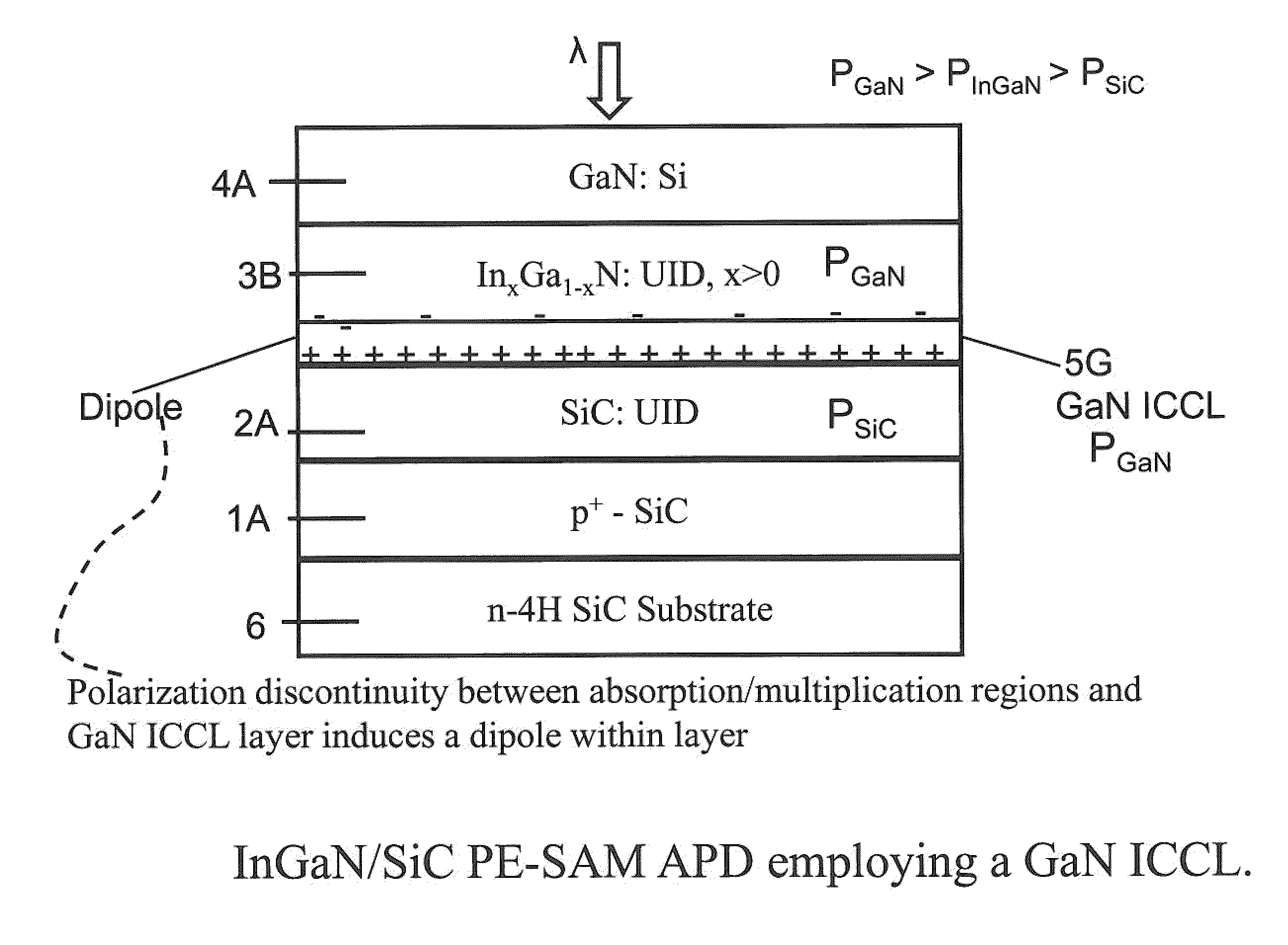
[0007]A preferred embodiment of the present invention comprises an avalanche
photodetector comprising a multiplication layer formed of a first material having a first polarization; the multiplication layer having a first electric field upon application of a bias
voltage; an absorption layer formed of a second material having a second polarization forming an interface with the multiplication layer; the absorption layer having a second electric field upon application of the bias voltage, the second electric field being less than the first electric field or substantially zero, carriers created by light absorbed in the absorption layer being multiplied in the multiplication layer due to the first electric field; the absorption layer having a second polarization which is greater or less than the first polarization to thereby create an interface charge; the interface charge being positive when the first material predominately multiplies holes, the interface charge being negative when the first material predominately multiplies electrons, the change in electric field at the interface occurring abruptly at the atomic level; the interface charge creating electric field discontinuity causing first electric field to attain the breakdown field in the multiplication region and the second electric field to be low or zero in the absorption layer to thereby eliminate the need for a doped
charge layer and the associated thickness of the doped charge layer required to transition from the low field to the
high field.
[0008]In a preferred embodiment, the
photodetector is an avalanche photodetector in which the need for a doped charge layer is eliminated, such that the transition from the low field in the absorption layer to the breakdown field in the multiplication layer occurs abruptly on the atomic scale at the interface and the required transition distance is eliminated resulting in only the minimum voltage being necessary to achieve the breakdown field required to trigger the
avalanche breakdown.
[0018]Another preferred embodiment photodetector comprises a photodetector that is a P-N
diode having an absorption layer comprising a
Group II or Group III polar n-type material and where the direction of vectors P1 and P2 are from multiplication layer towards the absorption layer and wherein the second polarization is greater than the first polarization and wherein the interface
charge control layer is doped with acceptors and the ionized acceptors create a negative
space charge that operates to effectively reduce the positive interface charge between the multiplication layer and the
charge control layer
[0022]A preferred method of forming an avalanche photodetector comprises providing a substrate; forming a first doped
semiconductor layer suitable for making electrical contact; forming a multiplication layer on the first doped
semiconductor layer; the multiplication layer having a first polarization; forming an interface
charge control layer on the multiplication layer, forming an absorption region on the interface charge
control layer; the absorption layer having a second polarization; the interface charge
control layer operating to create a field in the absorption layer, the interface charge
control layer operating to create a charge that enables a transition between the high electric field desired in the multiplication layer to ensure large
gain and the low electric field in the absorption layer to efficiently collect
photon generated carriers; forming a second doped semiconductor layer suitable for making electrical contact on the absorption layer. Optionally, the differential between the polarization of the absorption layer and polarization of the multiplication layer may be in excess of the product of the breakdown field and the
permittivity of the absorption layer relative to
free space, the interface charge control layer operating to create a field in the absorption layer by reducing the effective interface charge until it is less than the product the breakdown field of multiplication layer and the
permittivity of the absorption layer relative to
free space.
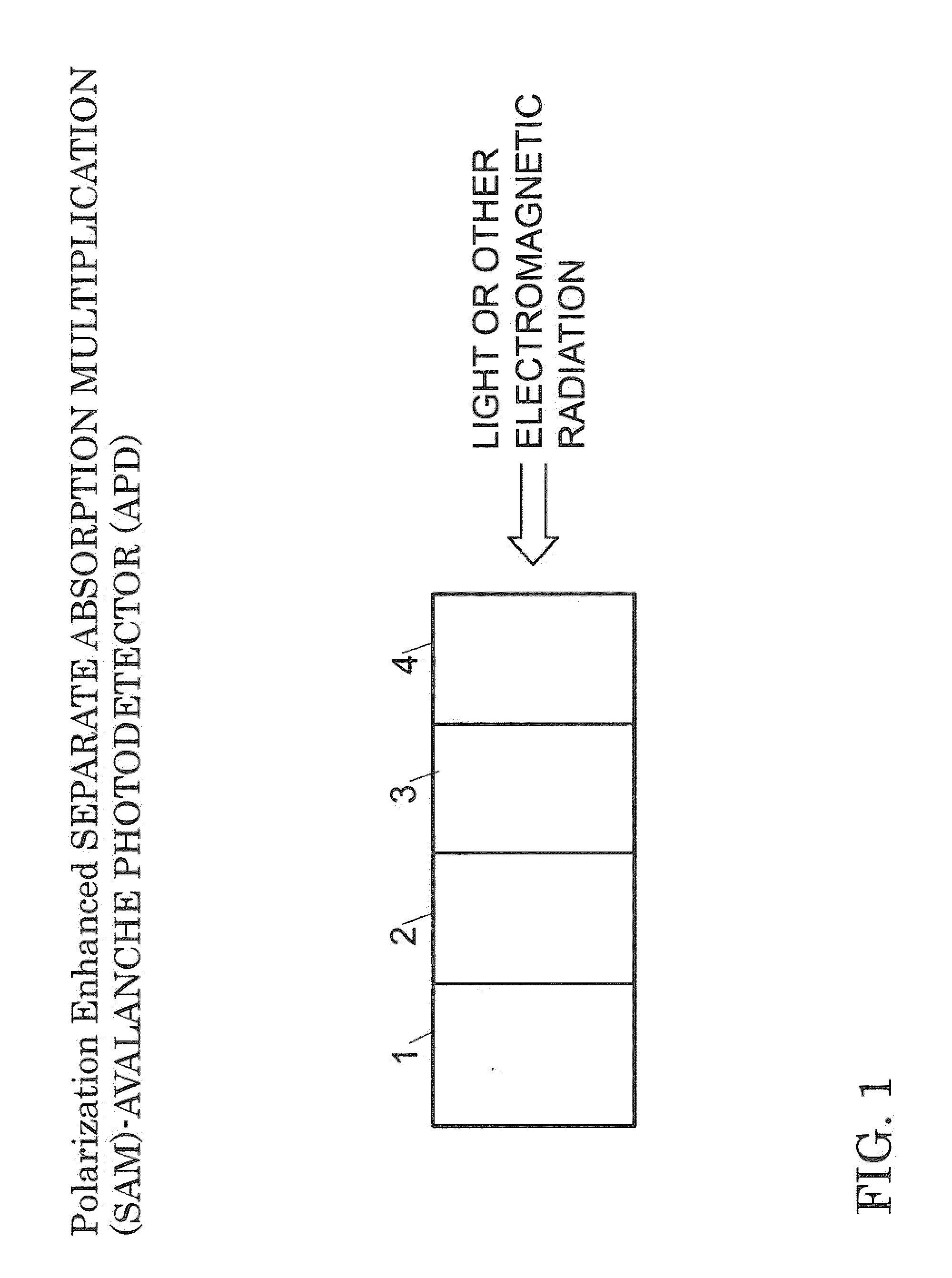
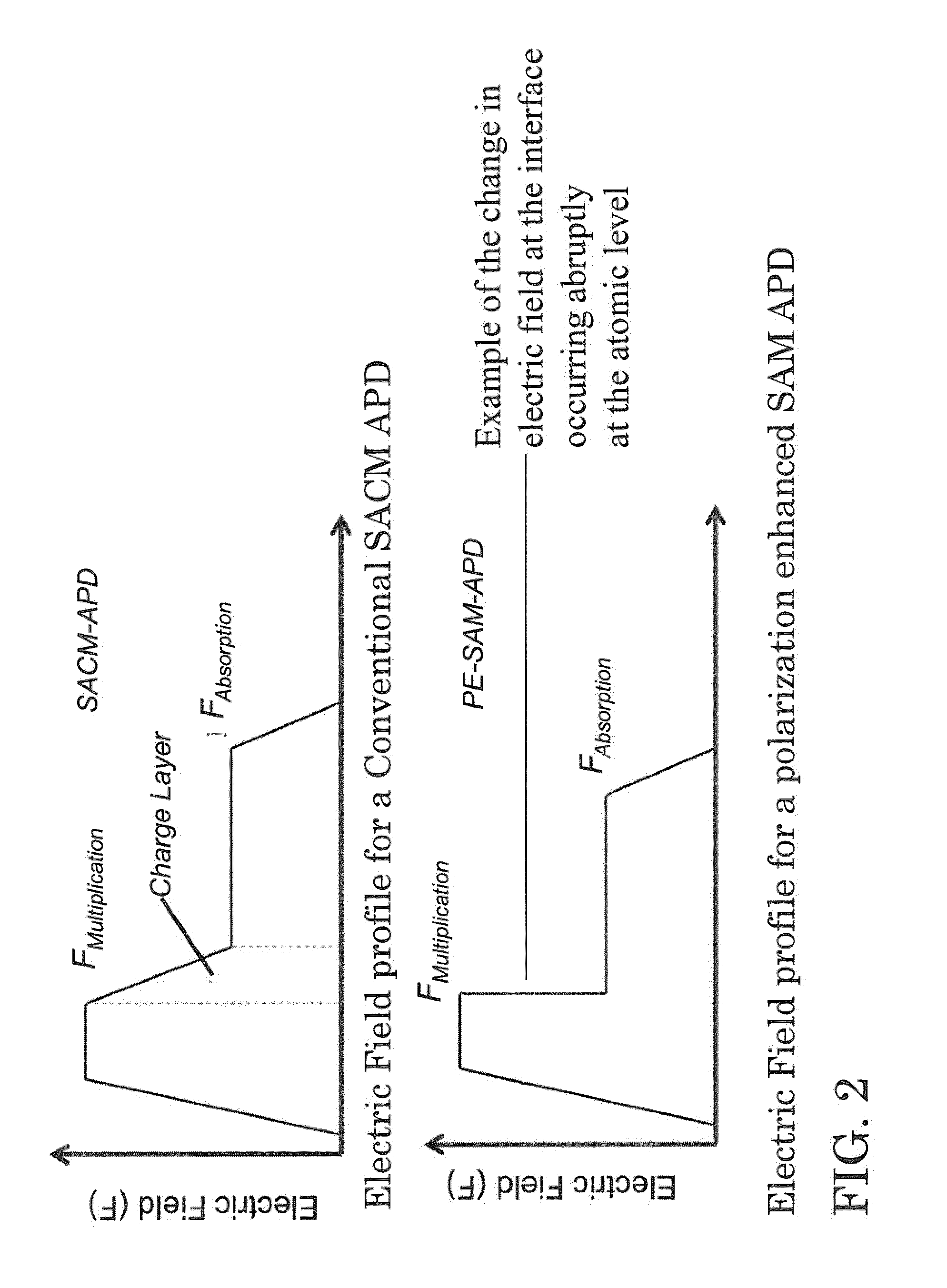
[0023]As shown in FIG. 1, the preferred embodiment illustrated comprises a multiplication
metal contact layer 1 and an absorption region
metal contact layer 4, a semiconductor absorption region (or layer) 3 having a total polarization P2 which is not equal to P1, and a semiconductor multiplication region (or layer) 2 having a total polarization P1. As shown in FIG. 2, this preferred embodiment device has the significant
advantage that the interface charge that arises due to the discontinuity in polarization at the interface between layer 2 and 3 enables a very sharp transition between the high electric field desired in the multiplication region to ensure large
gain and the low electric field desired in the absorption region to efficiently collect photogenerated carriers. As a result, this structure does not require a charge layer, and the significant voltage penalty associated with a charge layer, commonly employed in a separate absorption, charge and multiplication
avalanche photodiode (SACM-APD), to control the transition of the electric field from the multiplication to the absorption region (see FIG. 2 top).

