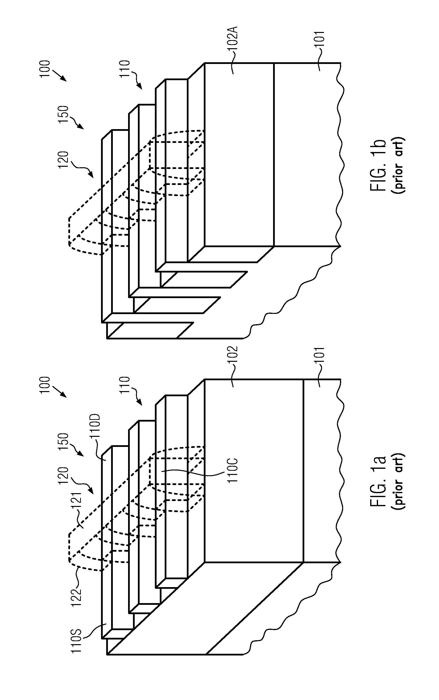
The short channel behavior may lead to an increased leakage current and to a dependence of the
threshold voltage on the channel length.
On the other hand, the three-dimensional nature of the
semiconductor fin comprising the channel region may result in additional
process complexity, for instance for patterning the gate
electrode structure, respective spacer elements and the like, wherein, additionally, compatibility with conventional planar
transistor architectures may be difficult to be achieved.
Moreover, conventional FinFET transistors may suffer from an increased
parasitic capacitance and, in particular, a moderately high
external resistance, i.e., a resistance for connecting to the drain and source regions, which may mainly be caused by the epitaxially grown additional drain and
source material for connecting the individual fin portions at the drain side and the source side of the FinFET transistor on the basis of highly complex epitaxial growth processes.
Furthermore, significant
dopant diffusion into the
buried oxide material may occur and may also contribute to inferior drive current capability of the semiconductor fins 110, even if provided with an intermediate epitaxially grown semiconductor material in the drain and source areas.
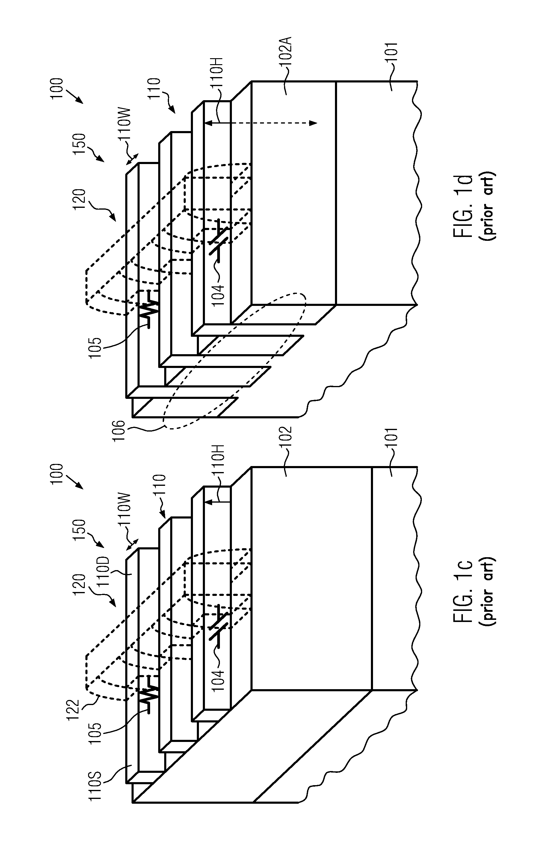
Any such strain-inducing mechanisms may be less efficient for the configuration as shown in FIG. 1c and thus other appropriate strain-inducing mechanisms may have to be developed.
Furthermore, embedded strain-inducing
semiconductor materials may generally have a reduced efficiency in SOI configurations, in particular when implemented in the FinFET as shown in FIG. 1c.
With respect to strain-inducing mechanisms, any overlying stressed
dielectric materials may also be significantly less efficient, comparable to the situation of the SOI configuration described above, while, on the other hand, any embedded strain-inducing semiconductor material may have a somewhat higher efficiency in the bulk configuration, however, with a generally very reduced effect.
Furthermore, highly complex epitaxial growth processes may be required to provide appropriate
contact resistance in the drain and source areas, which may nevertheless result in a moderately high
contact resistance.
Additionally, performance enhancing mechanisms, such as stressed
dielectric layers, embedded strain-inducing
semiconductor materials and the like, may be substantially non-effective, or may have a significantly reduced efficiency compared to planar transistor configurations and may thus require the new development of appropriate mechanisms.
Furthermore, conventional FinFET architectures may not be compatible with planar transistor architecture, or may at least require additional
process complexity for providing concurrently three-dimensional transistors and planar transistors.
For example, for SOI FinFETs, the required height of the semiconductor fins requires the provision of an appropriately thin semiconductor base material which, however, may be inappropriate for forming planar transistors, since a corresponding thickness of approximately 30 nm may not be appropriate for neither fully depleted planar transistors nor for partially depleted SOI transistors.

