Notwithstanding these advantages, ceramics have known drawbacks.
Tape cast varieties, however, are relatively expensive to fabricate and each comes with challenges in selecting compatibility relative to other materials.
Three, there exists a practical limitation in the sizes of substrates that can be fabricated due to corresponding limitations in the sizes of modern presses.
Naturally, this creates problems for manufacturers seeking to increase dimensions in printing swaths and chip arrays.
However, there remains limits and unresolved process challenges as will be seen.
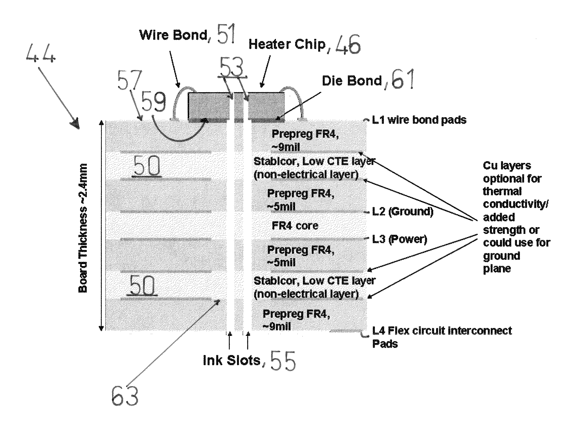
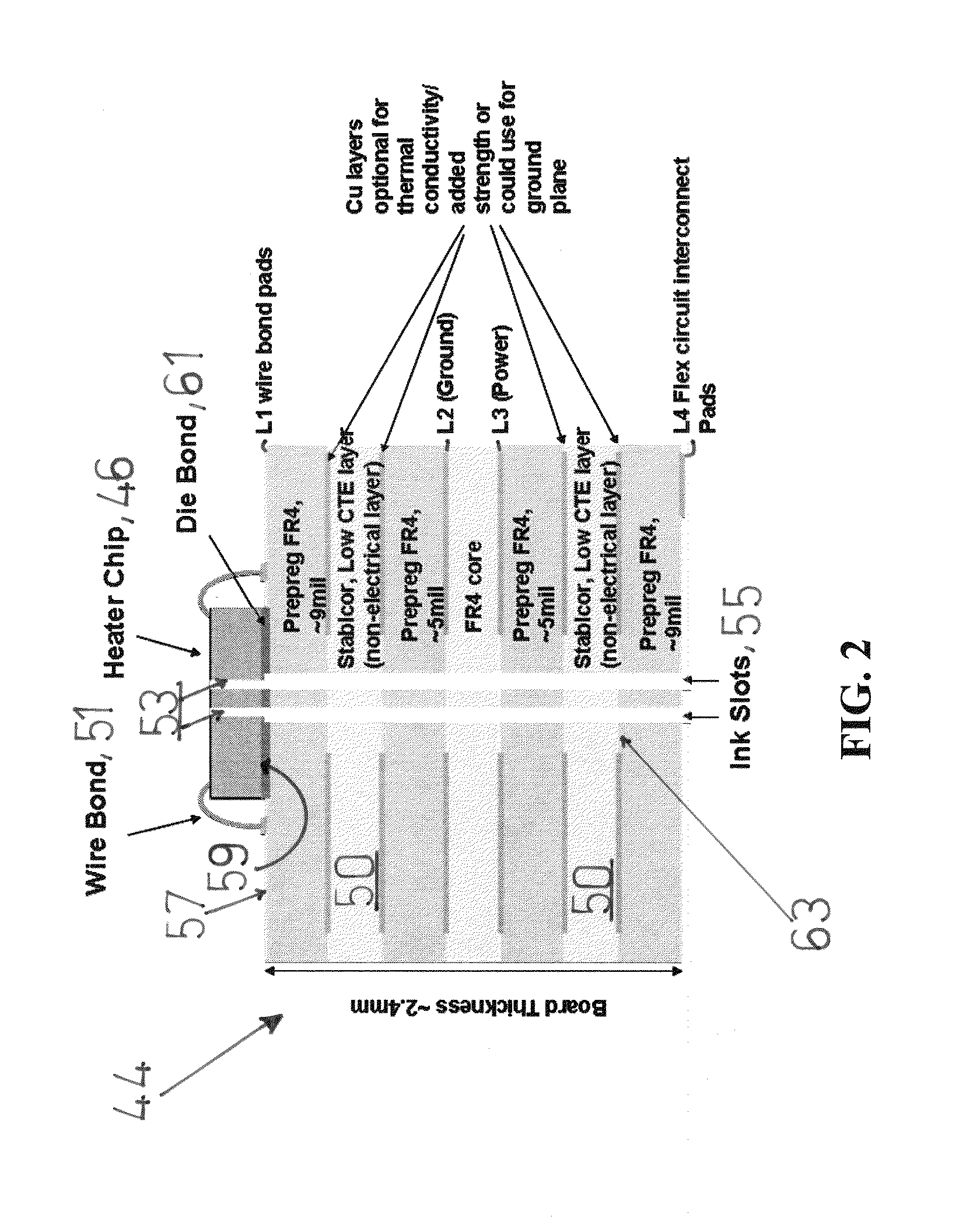
It also limits the space to add a protective FR4 layer to the bottom of the board, such as over trace areas so that the only exposed
metal on the bottom is for
flexible cable attachment pads.
By allowing a thicker die, on the other hand, the board thickness can increase but at an adverse cost to the substrate of poorer
thermal dissipation.
However, since the boards are thin and flexible, they tend to warp after fabrication.
This not only presents challenges for attaching the board to the
ceramic, but compromises
corrosion protection for the traces.
Still other problems associated with board-to-
ceramic attachment include: 1) squeezing
epoxy excesses into the chip pocket causing, thereby interfering with later die mounting or contributing to volume variability in the pocket and making encapsulation heights unpredictable; or 2) creating interfacial voids that allow ink to access the delicate wiring traces on the bottom of the board.
Alignment or registration between the board and ceramic has also resulted in manufacturing concerns.
One, the board warping makes it difficult to properly register components.
Two, routing tolerances on the board provide little room to adjust components.
As ejection heads move beyond single- or double-chip heads to larger arrays, the weight of now larger ceramics becomes problematic for smaller pick-and-place tools.
However,
UV curing lamps and other gluing fixtures are difficult to incorporate into standard tooling.
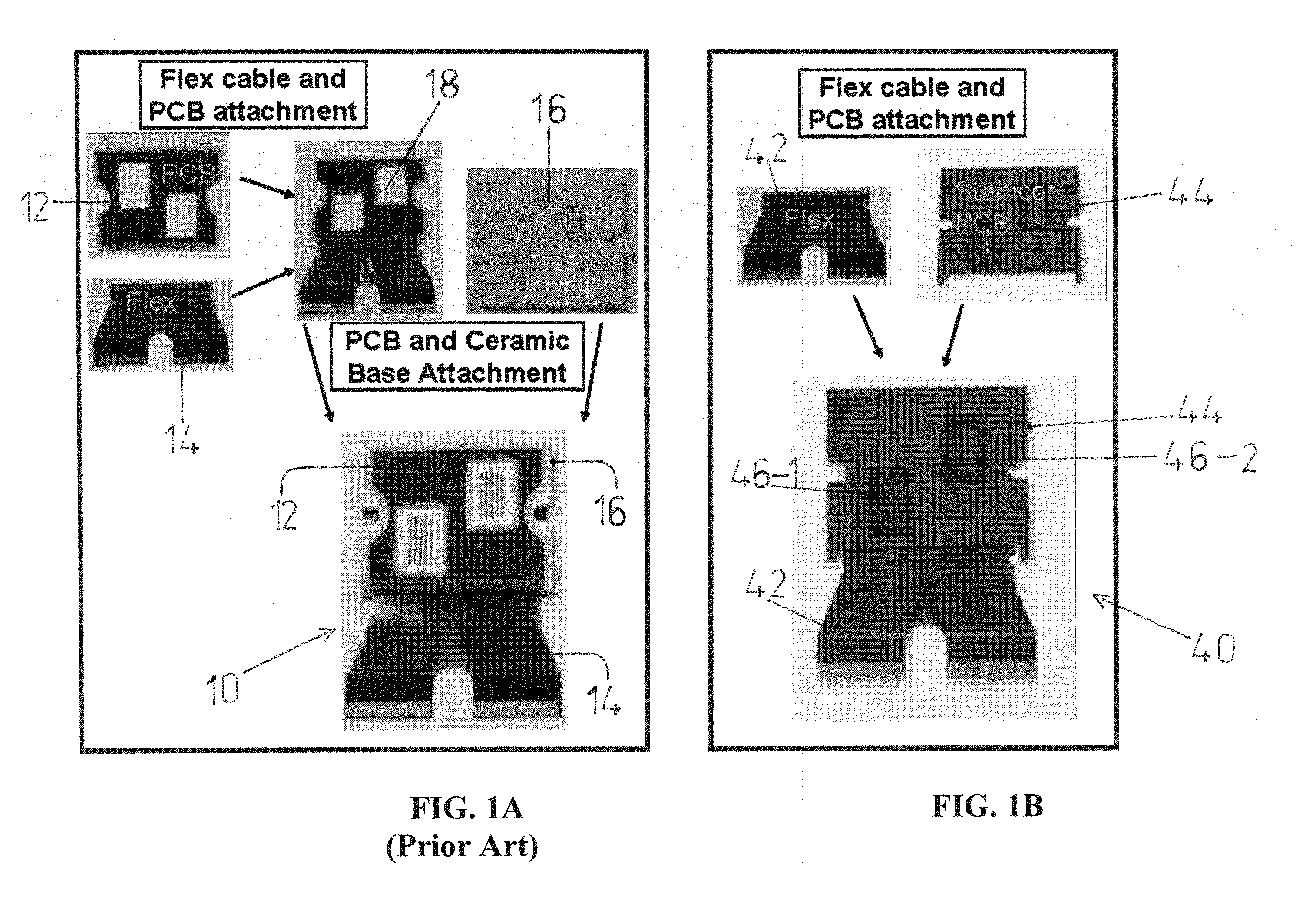
Neither of these, however, concern themselves with the challenges associated with precision methods needed to attach
silicon inkjet chips to PCB materials.
Rather, they relate to using conventional PCB material sets, which are insufficient for modern concerns.
Typical FR4 PCB materials, however, have CTEs of ˜16-20 ppm / ° C. and represent poor substrates for attachment to
silicon chips having CTEs of 2-4 ppm / ° C. While
ceramic materials with CTEs of 6-8 ppm / ° C. are a better match, they suffer the problems identified above.
Also, standard FR4 based circuit boards may not provide enough rigidity / stiffness for micro-fluid applications.
In turn, mounting a board
assembly to a printhead body can induce significant stresses that may translate into deformation where the die interfaces with the FR4 substrate.
˜25 W / mK), and this could prove challenging for dissipating heat generated during printing.
Unfortunately, the
printed circuit board 24 and ceramic base substrate 30 cause the design to encounter much of the same problems earlier described.

