Photomask and methods for manufacturing and correcting photomask

a manufacturing method and technology for masks, applied in the field of masks and photomask manufacturing methods, can solve the problems of difficulty in supplying pattern, and difficulty in mask production, so as to reduce mask costs, improve mask quality, and improve mask quality

Active Publication Date: 2011-12-01
DAI NIPPON PRINTING CO LTD
View PDF4 Cites 15 Cited by
  • Summary
  • Abstract
  • Description
  • Claims
  • Application Information

AI Technical Summary

Benefits of technology

[0060]According to a photomask of the present invention, in a halftone mask having an assist pattern, the formation of only the assist pattern part into a thin film allows a transferred image having high contrast to be formed while keeping the focal depth magnification effect as the assist pattern. Even though the assist pattern dimension is enlarged from 56 nm to 104 nm, the assist pattern part is not resolved and the focal depth magnification effect of a main pattern at a repetition end is not influenced badly and the assist pattern dimension may be enlarged to approximately twice the conventional dimension; the decreasing of an aspect ratio of the assist pattern produces the effect of restraining chip and falling of the assist pattern. Also, with regard to a photomask of the present invention, mask blanks for a halftone mask conventionally used may be directly used therefor in the case where a semi-transparent film is a single layer; the mask blanks material does not need to be modified, so that compatibility of the mask blanks may be secured in contrast to a halftone mask using no assist pattern, and quality maintenance of the mask and reduction of mask costs become feasible.
[0061]According to a manufacturing method of a photomask of the present invention, a main pattern and an assist pattern are each constituted from a semi-transparent film made of the same material, so that a film-forming process of the semi-transparent film is easy; mask blanks for a halftone mask conventionally used may be directly used therefor in the case where the semi-transparent film is a single layer, and the mask blanks material does not need to be modified, so that mask production costs may be reduced. A space between the main pattern and the assist pattern is widened so more by making the assist pattern width smaller than the main pattern as to allow a manufacturing method having a high margin of the misalignment of a first pattern formed on a transparent substrate with a second pattern formed subsequently, a

Problems solved by technology

However, in accordance with micronization of a semiconductor device pattern, a photomask having an assist pattern has had difficulty in producing the mask.
First, as described above, the difficulty is conceived to be such that the assist pattern itself needs not to be imaged on a wafer and needs to be minuter in dimension than a main pattern.
For example, in the case of forming a semiconductor device of a 65-nm line width on a wafer, the line width dimension of the main pattern on the mask (a reticle with an ordinary tetraploid pattern) is formed into approximately 200 nm to 400 nm in addition to optical proximity correction (OPC), while the line width dimension of the assist pattern becomes 120 nm or less and the mask production becomes extr

Method used


Image

  • Photomask and methods for manufacturing and correcting photomask
  • Photomask and methods for manufacturing and correcting photomask
  • Photomask and methods for manufacturing and correcting photomask

Examples


first embodiment

[0139]Thus, a manufacturing method of a photomask of the present invention is a manufacturing method for solving the above-mentioned problems, and a manufacturing method of a photomask which uses an ArF excimer laser as an exposing source, is used for a projection exposure by an off axis illumination, and is provided on a transparent substrate with a main pattern to be transferred to a transfer-target surface by a projection exposure and an assist pattern to be formed nearby the main pattern and not transferred to a transfer-target surface.

[0140]FIGS. 7A to 7E is a process cross-sectional schematic view showing a first embodiment of a manufacturing method of a photomask of the present invention shown in FIG. 1. As shown in FIG. 7A, a semi-transparent film 72 is formed on a transparent substrate 71 such as a synthetic quartz substrate to obtain film thickness for allowing a retardation of approximately 180° between the light transmitting through the semi-transparent film 72 and the l...

second embodiment

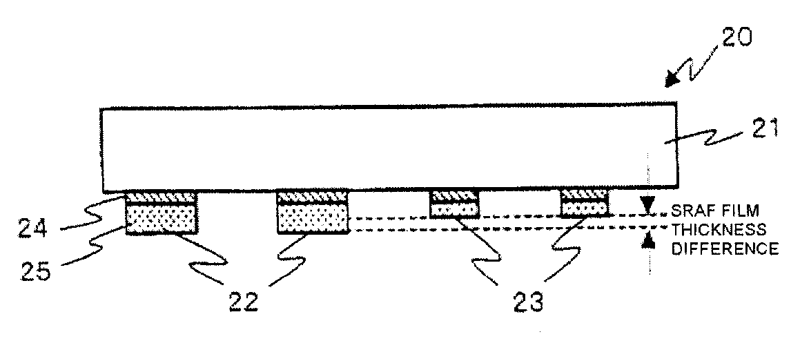
[0150]FIGS. 8A to 8E are a process cross-sectional schematic view showing a second embodiment of a manufacturing method of a photomask of the present invention shown in FIG. 1; similarly to FIG. 7A, a semi-transparent film 82 is formed on a transparent substrate 81 to obtain film thickness for allowing a retardation of approximately 180° between the light transmitting through the semi-transparent film 82 and the light transmitting through a transparent region of the transparent substrate 81, and subsequently prepare photomask blanks such that a light shielding film 83 is formed on the above-mentioned semi-transparent film (FIG. 8A).

[0151]Next, a first resist pattern 84 is formed on the light shielding film 83, and the light shielding film 83 and the semi-transparent film 82 are sequentially dry-etched to stop etching in the halfway stage of half-etching the semi-transparent film 82. In this stage, a thin layer of the semi-transparent film 82 to be removed remains partially on the tr...

third embodiment

[0156]FIGS. 9A to 9F are a process cross-sectional schematic view showing an embodiment of a manufacturing method of a photomask of the present invention shown in FIG. 2. As shown in FIG. 9A, a semi-transparent film 92a and a semi-transparent film 92 are sequentially formed on a transparent substrate 91 such as a synthetic quartz substrate to form a two-layer semi-transparent film. The lower-layer semi-transparent film 92a has the function of an etch stop layer during dry-etching of the upper-layer semi-transparent film 92 and also has the function as a mask material for a semi-transparent film. The film thickness for allowing a retardation of approximately 180° between the light transmitting through the two-layer semi-transparent film and the light transmitting through a transparent region of the transparent substrate 91 is obtained to subsequently prepare photomask blanks such that a light shielding film 93 is formed on the above-mentioned two-layer semi-transparent film.

[0157]A c...


PUM


Abstract

The present invention provides a halftone mask comprising an assist pattern and a manufacturing method of the halftone mask, which uses an ArF excimer laser as an exposing source, is used for a projection exposure by an off axis illumination, does not resolve the assist pattern while keeping the focal depth magnification effect as the assist pattern, and may form a transferred image having high contrast of a main pattern. A photomask is a photomask comprising the main pattern which is transferred to a transfer-target surface by the projection exposure and the assist pattern which is formed nearby the main pattern and not transferred, characterized in that the main pattern and the assist pattern are each constituted from a semi-transparent film made of the same material, a retardation of 180° is generated between the light transmitting through the main pattern and the light transmitting through a transparent region of a transparent substrate, and a predetermined retardation within the scope of 70° to 115° is generated between the light transmitting through the assist pattern and the light transmitting through the transparent region of the transparent substrate.

Description

TECHNICAL FIELD[0001]The present invention relates to a photomask and a manufacturing method of the photomask, which is used for a photolithographic technique using a shortwave exposing source such as an excimer laser exposure device used for patterning a semiconductor device, and a correcting method of the photomask and the corrected photomask, and particularly relates to a halftone photomask and a manufacturing method of the halftone photomask, in which an assist pattern is disposed nearby a main pattern, and a correcting method of the photomask and the corrected photomask.BACKGROUND ART[0002]In order to realize high integration and ultramicronization of a semiconductor device developing from a half pitch of 65 nm into 45 nm and further 32 nm, a high-NA technique for increasing the numeric aperture of a projector lens, an immersion exposure technique for exposing while making a high-refraction medium intervene between a projector lens and an exposure target, and an off axis illumi...

Claims


Application Information

Patent Timeline
IPC IPC(8): G03F1/14G03F1/00G03F1/36
CPCG03F1/144G03F1/32G03F1/72G03F1/0076G03F1/0092G03F1/36G03F1/28G03F1/44G03F1/20G03F1/68H01L21/0274G03F1/30G03F1/38G03F1/80
Inventor NAGAI, TAKAHARUTAKAMIZAWA, HIDEYOSHIMOHRI, HIROSHIMORIKAWA, YASUTAKAHAYANO, KATSUYA
Owner DAI NIPPON PRINTING CO LTD
Why Eureka
Try Eureka