Method for the Manufacture of Double-Sided Metallized Ceramic Substrates

a technology of metallized ceramics and substrates, applied in the direction of electrical appliances, domestic applications, applications, etc., can solve the problems of metal plates to the top and underside of ceramics, damage to metal-ceramic substrates, time-consuming and costly, etc., and achieve the effect of simple and economically-implementable methods

Active Publication Date: 2011-12-15
IXYS SEMICON
View PDF2 Cites 6 Cited by
  • Summary
  • Abstract
  • Description
  • Claims
  • Application Information

AI Technical Summary

Benefits of technology

[0016]The invention is provides a simple and economically-implementable method for the manufacture of double-sided metallized metal-ceramic substrates using a direct-bonding process

Problems solved by technology

With the method of U.S. Pat. No. 3,994,430, there is the disadvantage that the bonding of the metal plates to the top and underside of the ceramic because with simultaneous bonding of both metal plates, the lower metal plate tends to adhere to the substrate carrier, and the subsequent detachment leads to damage of the metal-ceramic substrate.
This is time-consuming and costly.
The disadvantage is that the separation layer required must first to be applied with suitable means, and after the bonding process, must be removed from the metal surface with a suitable process.
This approach also involves additional time and cost.
A further problem with the joining of metal-ceramic substrates by means of a liquid-phase bonding process lies in the fact that the bonding between the metal plate and the ceramic substrate does not take place across the entire surface.
The incl

Method used


Image

  • Method for the Manufacture of Double-Sided Metallized Ceramic Substrates
  • Method for the Manufacture of Double-Sided Metallized Ceramic Substrates
  • Method for the Manufacture of Double-Sided Metallized Ceramic Substrates

Examples


Embodiment Construction

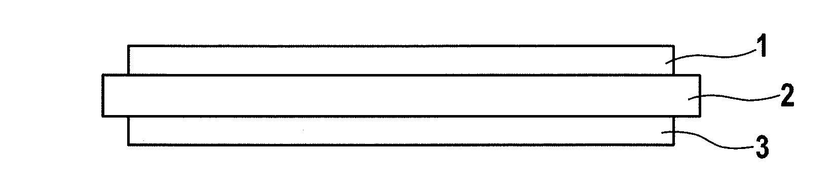
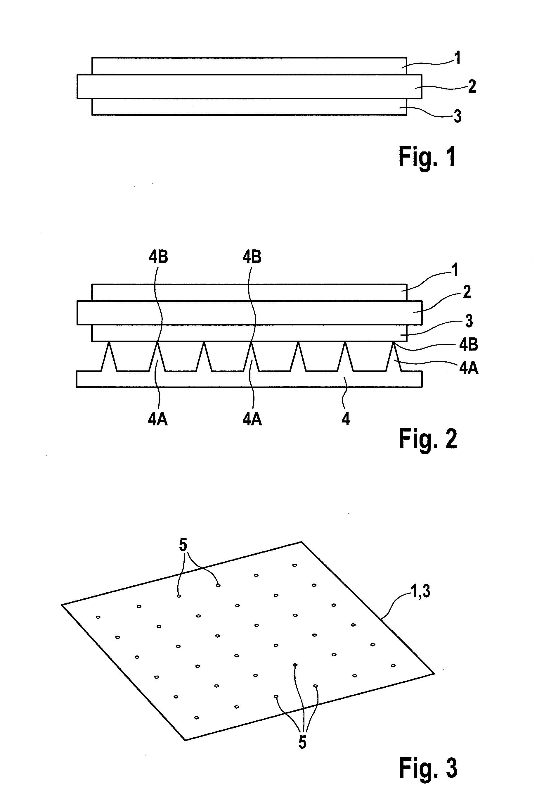
[0033]FIG. 1 shows an arrangement, formed as a DCB package, consisting of a first top metal plate 1 and a second bottom metal plate 3, between which is located a ceramic substrate 2. The metal plates 1, 2, are copper plates or foils respectively. The ceramic substrate is an oxide ceramic substrate, in particular an aluminium oxide ceramic.

[0034]The method known as the direct-bonding process, for the bonding of the oxidized metal plates 1 and 3 to the ceramic substrate 2 is described in detail in EP 0085914, to which reference is expressly made.

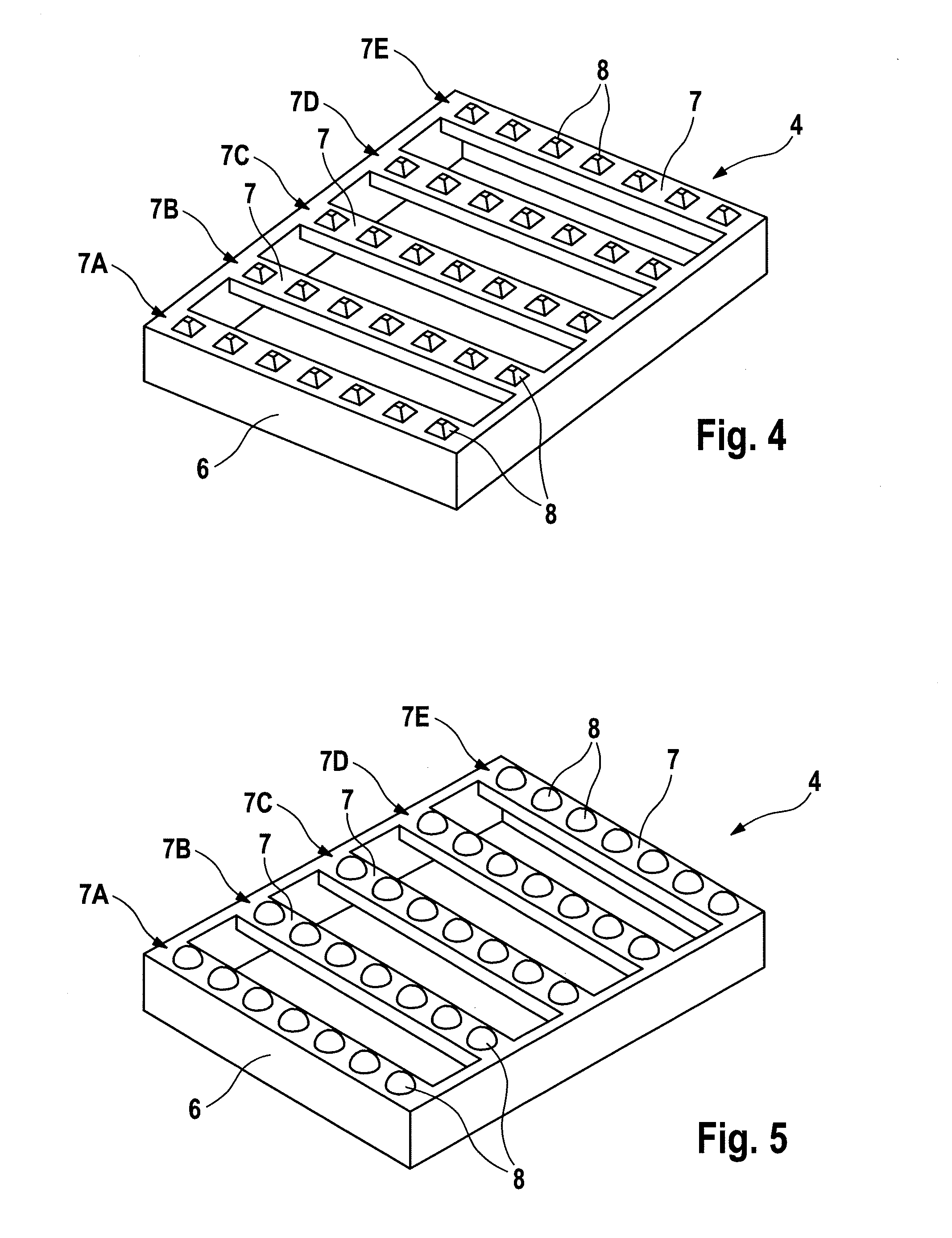
[0035]The method according to the invention is characterized in that the DCB package is laid on a specially structured carrier 4 (FIG. 2). The carrier 4 is a plate of at least one of the compounds selected from the group consisting of mullite, aluminium nitride, boron nitride, silicon nitride, zirconium nitride, silicon carbide, and graphite. The plate exhibits on the upper side, which faces towards the DCB package 1, 2, 3, a plurality of proj...


PUM

PropertyMeasurementUnit
Diameteraaaaaaaaaa
Diameteraaaaaaaaaa
Diameteraaaaaaaaaa

Abstract

The invention relates to a method for the manufacture of double-sided metallized ceramic substrates according to the direct-bonding process. The method enables a ceramic substrate to be bonded to a metal plate or foil on the upper side and the underside in only one process sequence. The composite to be bonded is located on a specially designed carrier structured on the upper side with a plurality of contact points. After the bonding process the composite of metal plates and ceramic substrate can be detached from the carrier free of any residue.

Description

CROSS-REFERENCE TO RELATED APPLICATION[0001]This application claims priority from German Patent Application No. 10 2010 023 637.3, filed Jun. 14, 2010, which is incorporated herein by reference for all purposes.BACKGROUND OF THE INVENTION[0002]The invention relates to a method for the manufacture of double-sided metallized ceramic substrates according to a direct-bonding process. Double-sided metallized ceramic substrates are generally known. Such metal-ceramic substrates are particularly useful for power semiconductor modules as circuit carriers. These circuit carriers include a top and underside with a ceramic provided with a Cu-metallization, with at least one metallized side having a circuitry structure. The known method for the manufacture of these metal-ceramic composites, by means of eutectic bonding, is generally understood as direct-bonding process or Direct Copper Bonding (“DCB”).[0003]U.S. Pat. No. 3,994,430 and EP 0 085 914 describe a method for the manufacture of metal-...

Claims


Application Information

Patent Timeline
IPC IPC(8): C04B37/02
CPCC04B37/021H05K2203/016C04B2235/9623C04B2237/06C04B2237/341C04B2237/407C04B2237/54C04B2237/56C04B2237/561C04B2237/568C04B2237/62C04B2237/704H05K1/0306H05K3/007H05K3/385C04B37/025H01L23/15H01L23/48H01L23/492H05K1/09
Inventor WEIDENAUER, WERNERSPANN, THOMASKNOLL, HEIKO
Owner IXYS SEMICON
Why Eureka
Try Eureka