Bi-directional switch, alternating-current two-wire switch, switching power source circuit, and method of driving bi-directional switch

a technology of alternating-current two-wire switch and bi-directional switch, which is applied in the direction of electronic switching, pulse generator, pulse technique, etc., can solve the problem of inability to ignore heat, and achieve the effects of reducing conduction losses, low on-resistance, and high mobility

Active Publication Date: 2011-12-15
PANASONIC CORP
View PDF2 Cites 29 Cited by
  • Summary
  • Abstract
  • Description
  • Claims
  • Application Information

AI Technical Summary

Benefits of technology

[0008]In recent years, introduction of Group-III nitride semiconductors represented by GaN or semiconductor devices using a wide-gap semiconductor such as silicon carbide (SiC) has been considered with an aim to reduce conduction losses by breaking material limits. A wide-gap semiconductor has a breakdown electric field higher than that of Si by about one digit. Due to a spontaneous polarization and a Piezo polarization, charge occurs at the hetero junction interface between aluminum gallium nitride (AlGaN) and gallium nitride. In this way, a two-dimensional electron gas (2 DEG) layer is formed which has a sheet carrier concentration of 1×1013 cm−2 or higher and a high mobility of 1000 cm2 V / sec or higher even when it is undoped. For this reason, such AlGaN / GaN hetero junction field effect transistor (AlGaN / GaN-HFET) is expected as a power switching transistor which achieves a low on-resistance and a high voltage resistance.
[0009]In particular, it is possible to form a bi-directional semiconductor device using a single semiconductor device by configuring it to have two gate electrodes using such an AlGaN / GaN hetero junction (for example, see Patent Reference 2 (International Publication No. 2008 / 062800)). Furthermore, the bi-directional semiconductor device configured as mentioned above is a circuit equivalent to two transistors connected in series in mutually opposite directions, and thus is capable of reducing the on-resistance more significantly. Therefore, the bi-directional semiconductor device is capable of controlling not only current that flows from a first electrode side to a second electrode side but also current that flows from the second electrode side to the first electrode side. For this reason, with the bi-directional semiconductor device, it is possible to achieve miniaturization and electric power reduction more significantly than in the case of using a conventional bi-directional semiconductor device obtained by combining a triac element used as a bi-directional switch, and a power transistor that is either a power MOSFET (a metal oxide semiconductor field effect transistor) or an IGBT (insulated gate bipolar transistor).

Problems solved by technology

Furthermore, since the MOSFETs and diodes are inserted in the power source line, it is impossible to ignore heat caused thereby.

Method used


Image

  • Bi-directional switch, alternating-current two-wire switch, switching power source circuit, and method of driving bi-directional switch
  • Bi-directional switch, alternating-current two-wire switch, switching power source circuit, and method of driving bi-directional switch
  • Bi-directional switch, alternating-current two-wire switch, switching power source circuit, and method of driving bi-directional switch

Examples


embodiment 1

Variation of Embodiment 1

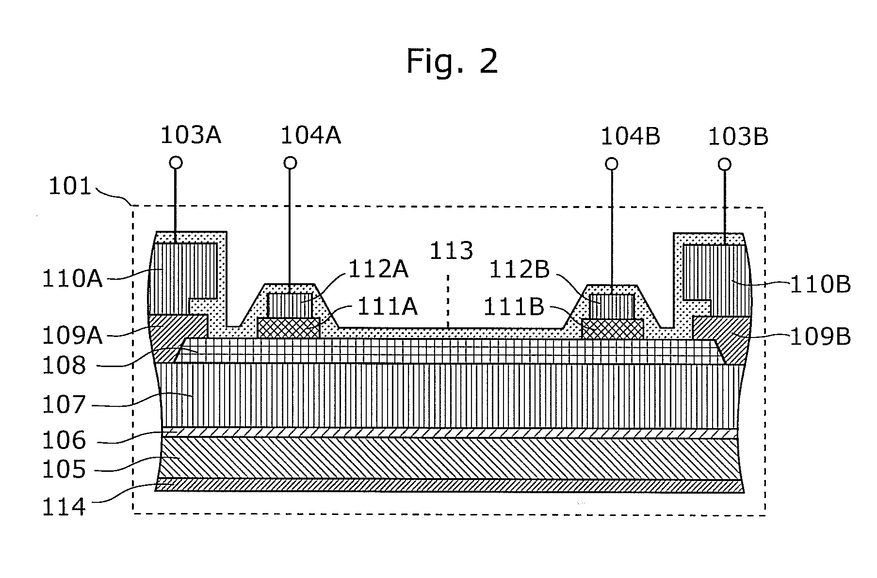
[0098]Variation of Embodiment 1 is described with reference to the drawings. FIG. 11 is a block diagram showing a structure of a bi-directional switch 10 in this variation of Embodiment 1. FIG. 12 is a cross-sectional view of the semiconductor device 101 in this variation of Embodiment 1. The same structural elements as in Embodiment 1 are assigned with the same numerical references, and no detailed descriptions thereof are repeated.

[0099]As shown in FIG. 12, the semiconductor device 101 according to this variation of Embodiment 1 has a back surface electrode 114 connected to a substrate terminal 115. As shown in FIG. 11, the control unit 102 further includes a substrate potential control unit 102b which controls the potential of the substrate terminal 115 for the semiconductor device 101, in addition to the operation mode control unit 102a which controls the first control terminal 104A and the second control terminal 104B of the semiconductor device 101.

[01...

embodiment 2

Variation of Embodiment 2

[0117]An alternating-current two-wire switch according to Variation of Embodiment 2 is described with reference to the drawings. FIG. 15 is a block diagram of the alternating-current two-wire switch according to Variation of Embodiment 2. In the alternating-current two-wire switch according to this variation of Embodiment 2, the semiconductor device 201 has a back surface electrode 114 connected to a substrate terminal 115. Furthermore, the control unit 202 includes a substrate potential control unit 206 that controls the potential of the substrate terminal 115.

[0118]As with the IS2S1-VS2S1 characteristics of the semiconductor device according to Variation of Embodiment 1, the semiconductor device 201 operates in a state where the on-resistance is large, in the case where a negative voltage is applied as a substrate voltage. Accordingly, it is possible to reduce the amount of an inrush current at the time when the alternating-current two-wire switch is activ...

embodiment 3

Variation of Embodiment 3

[0129]A switching power source circuit according to Embodiment 3 is described with reference to the drawings. FIG. 17 is a block diagram of the switching power source circuit according to Variation of Embodiment 3. In the switching power source circuit according to Variation of Embodiment 3, the semiconductor device 301 has a back surface electrode 114 connected to a substrate terminal 115. Furthermore, the control unit 302 includes a substrate potential control unit 306 that controls the potential of the substrate terminal 115.

[0130]As with the IS2S1-VS2S1 characteristics of the semiconductor device according to Variation of Embodiment 1, the semiconductor device 301 operates in a state where the on-resistance is large, in the case where a negative voltage is applied as a substrate voltage. Accordingly, it is possible to reduce the amount of an inrush current at the time when the switching power source circuit is activated.

[0131]The present invention has be...


PUM


Abstract

A semiconductor device 101 in a bi-directional switch includes: a first electrode 109A, a second electrode 109B, a first gate electrode 112A, and a second gate electrode 112B. In a transition period: when the potential of the first electrode 109A is higher than the potential of the second electrode 109B, a voltage lower than the first threshold voltage is applied to the first gate electrode 112A and a voltage higher than the second threshold value voltage is applied to the second gate electrode 112B; and otherwise, a voltage higher than the first threshold value voltage is applied to the first gate electrode, and a voltage lower than the second threshold value voltage is applied to the second gate electrode.

Description

BACKGROUND OF THE INVENTION[0001](1) Field of the Invention[0002]The present invention relates to bi-directional switches, and in particular to (A) a bi-directional switch which (i) includes a semiconductor device including Group-III nitride semiconductor and materials, (ii) is intended for protection against an inrush current, and (iii) is for use in an alternating-current two-wire switch, a switching power source circuit, and the like, (B) the alternating-current two-wire switch circuit, the switching power source, and the like that include the bi-directional switch, and (C) a method of driving the bi-directional switch.[0003](2) Description of the Related Art[0004]With the recent application of inverter techniques to electric devices, inrush currents that occur at the time when such electric devices are activated may increase electromagnetic interference to nearby electric appliances and loads on the electric devices themselves. At the time of the activation, a large current flow...

Claims


Application Information

Patent Timeline
Patent Type & Authority Applications(United States)
IPC IPC(8): H02M7/02H03K17/94H03K17/687
CPCH01L29/2003H01L29/42316H03K2217/0009H03K17/6871H03K2017/6875H01L29/7787
Inventor YAMAGIWA, HIROTOHASHIZUME, SHINGOYANAGIHARA, MANABUIKOSHI, AYANORI
Owner PANASONIC CORP
Why Eureka
Try Eureka