Semiconductor device and method for driving the same

a semiconductor device and semiconductor technology, applied in semiconductor devices, digital storage, instruments, etc., can solve the problems of increasing the cost per storage capacity, difficult to sufficiently reduce the power consumption of the storage element, and short data retention time, so as to achieve the effect of reducing the area of the semiconductor device, facilitating data storage, and increasing the integration

Inactive Publication Date: 2011-12-29
SEMICON ENERGY LAB CO LTD
View PDF11 Cites 14 Cited by
  • Summary
  • Abstract
  • Description
  • Claims
  • Application Information

AI Technical Summary

Benefits of technology

[0030]According to one embodiment of the present invention, the area of a semiconductor device can be reduced; thus, a semiconductor device with higher integration and larger storage capacity can be provided.
[0031]In addition, deterioration of a gate insulating layer hardly occurs because data writing does not need high voltage; thus, the number of write cycles and the reliability are greatly increased.
[0032]Further, an operation for erasing data is not needed, so that high-speed operation can be easily realized.
[0033]Data is stored by making an oxide semiconductor an insulator, so that the stored data can be retained for an extremely long time. In other words, a refresh operation becomes unnecessary or the frequency of refresh operations can be extremely low. Consequently, power consumption of the semiconductor device can be reduced. Moreover, stored data can be retained for a long time even when power is not supplied.

Problems solved by technology

Moreover, a transistor included in a storage element has a leakage current and electric charge flows into or out of a capacitor even when the transistor is not selected, so that the data retention time is short.
For that reason, another write operation (refresh operation) is necessary at predetermined intervals, and it is difficult to sufficiently reduce power consumption of the storage element.
Furthermore, since stored data is lost when power supply stops, an additional storage device using a magnetic material or an optical material is needed in order to hold the data for a long time.
However, cost per storage capacity is increased because of the use of a flip-flop or the like.
Moreover, as in a DRAM, stored data in an SRAM is lost when power supply stops.
However, a gate insulating layer included in a storage element deteriorates by tunneling current generated in writing, so that the storage element stops its function after a limited number of write operations.
Moreover, employing such a method does not solve the fundamental problem of lifetime.
In other words, a flash memory is not suitable for applications in which data is frequently rewritten.
Further, it takes a relatively long time to perform an operation for injecting or removing electric charge, so that it is not easy to increase the speed of write and erase operations.

Method used


Image

  • Semiconductor device and method for driving the same
  • Semiconductor device and method for driving the same
  • Semiconductor device and method for driving the same

Examples


embodiment 1

[0052]In this embodiment, an example of a circuit configuration and an operation of a semiconductor device according to one embodiment of the disclosed invention will be described with reference to FIGS. 1A and 1B, FIGS. 2A and 2B, FIGS. 3A and 3B, and FIG. 4. In this embodiment, the case where an n-channel transistor (n-type transistor) is used will be described.

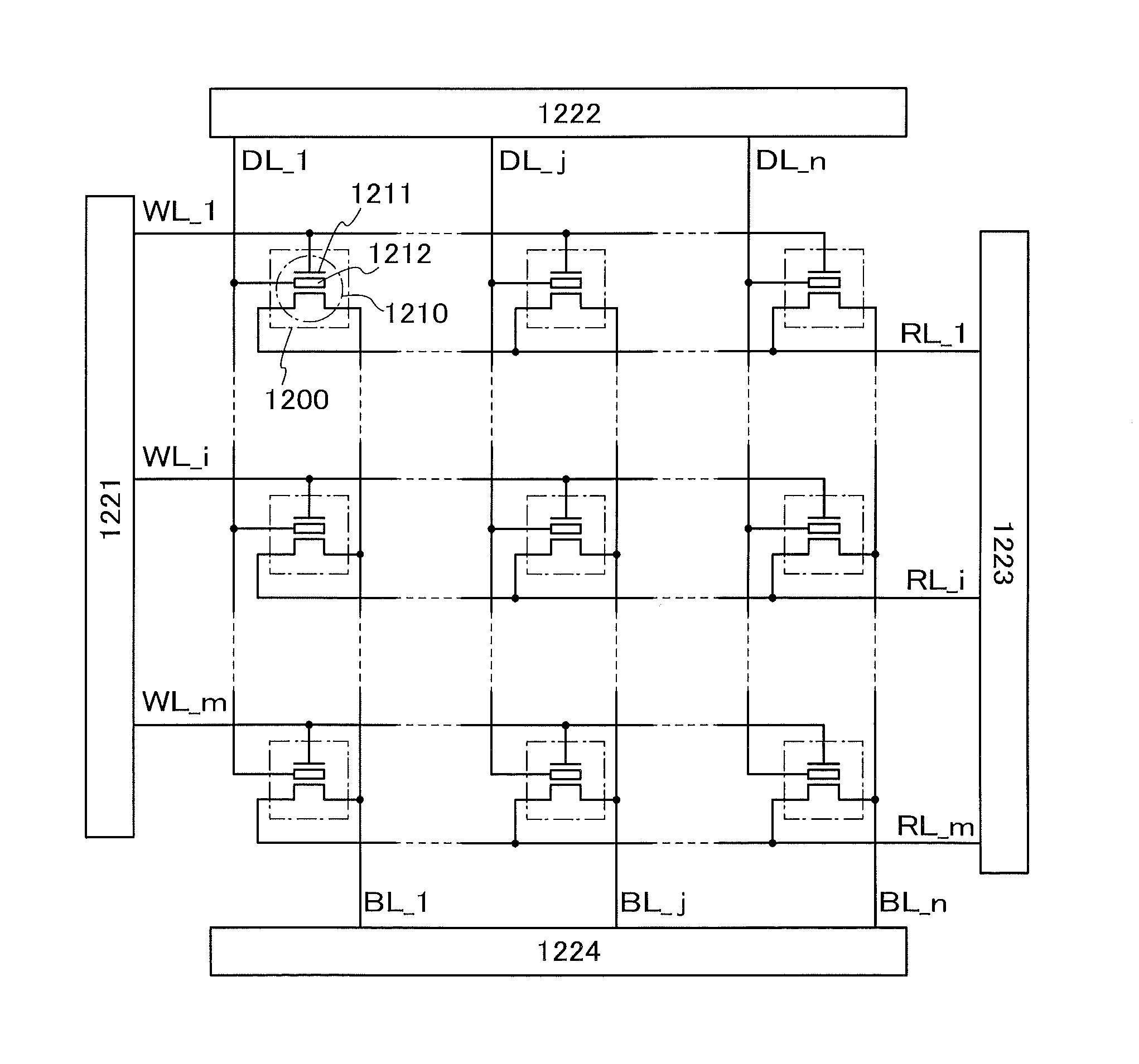
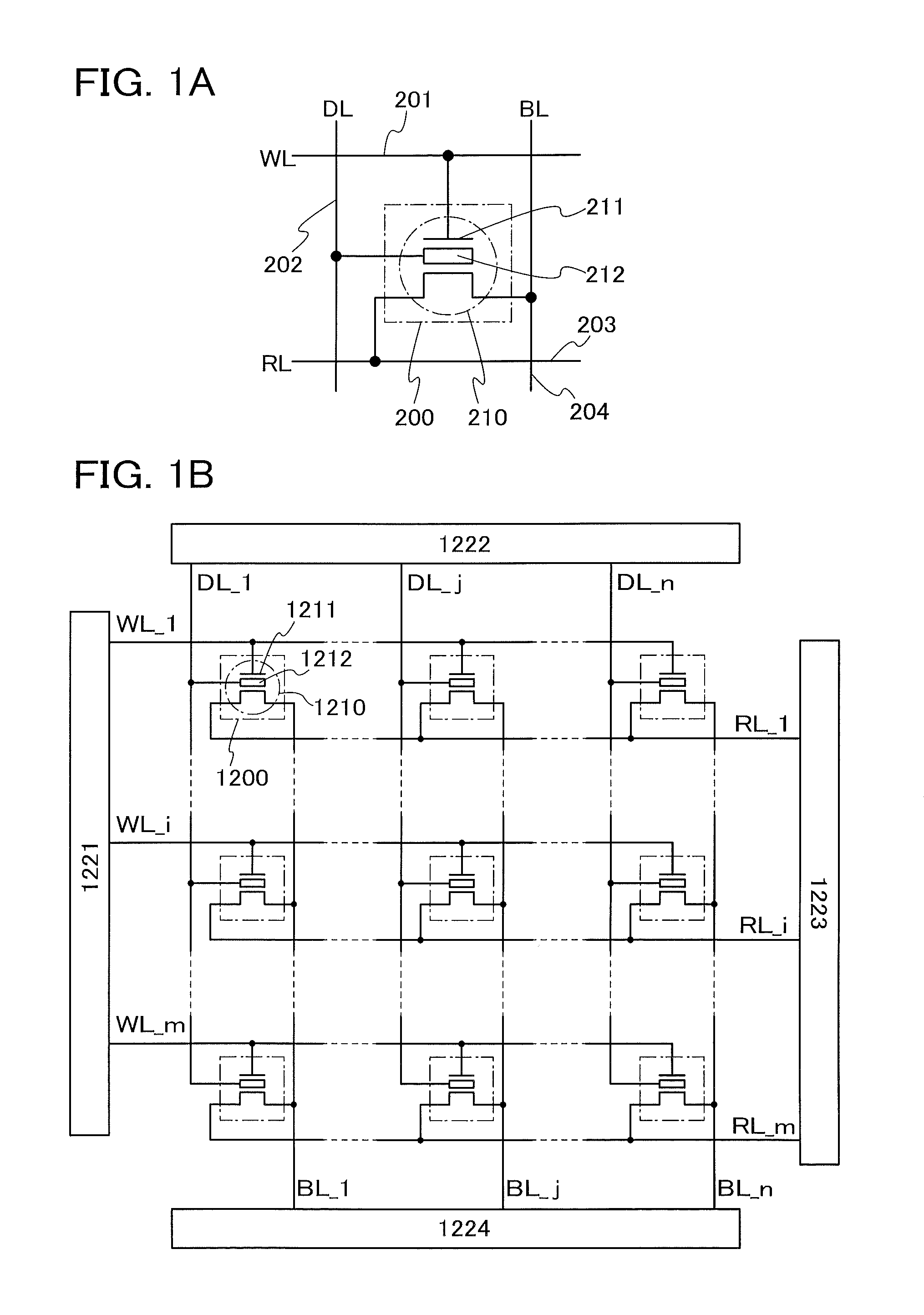
[0053]FIG. 1A illustrates a circuit configuration of a non-volatile memory cell 200 including a transistor 210. The transistor 210 has a control gate 211 and a storage gate 212. In FIG. 1A, the control gate 211 of the transistor 210 is electrically connected to a first wiring 201 (also referred to as a word line WL). The storage gate 212 of the transistor 210 is electrically connected to a second wiring 202 (also referred to as a data line DL). One of a source and a drain of the transistor 210 is electrically connected to a third wiring 203 (also referred to as a read signal line RL). The other of the source and the drain o...

embodiment 2

[0125]In this embodiment, an example of a structure and a manufacturing method of the semiconductor device described in Embodiment 1 will be described with reference to FIGS. 5A to 5C, FIGS. 6A to 6D, and FIGS. 7A and 7B.

[0126]FIGS. 5A to 5C illustrate an example of a transistor 150 that can be used as a storage element. FIG. 5A illustrates a planar structure of the transistor 150. FIG. 5B illustrates a cross section along X1-X2 in FIG. 5A. FIG. 5C is an enlarged view of a portion 180 in FIG. 5B.

[0127]In the transistor 150, a base insulating layer 110 is provided over a substrate 100. A control gate 101 is provided over the base insulating layer 110. A first gate insulating layer 102 is provided over the control gate 101. An electrode 103 is provided over the first gate insulating layer 102. A storage gate 104 is provided in contact with the first gate insulating layer 102 and the electrode 103. A second gate insulating layer 105 is provided over the storage gate 104. A semiconducto...

embodiment 3

[0208]In this embodiment, examples of an electronic device to which the semiconductor device described in the above embodiment is applied will be described with reference to FIGS. 8A to 8F. Specifically, this embodiment explain applications of the semiconductor device described in the above embodiment to electronic devices such as a computer, a mobile phone handset (also referred to as a mobile phone or a mobile phone device), a personal digital assistant (including a portable game machine and an audio reproducing device), a camera such as a digital camera and a digital video camera, electronic paper, and a television device (also referred to as a television or a television receiver).

[0209]FIG. 8A illustrates a laptop personal computer including a housing 701, a housing 702, a display portion 703, a keyboard 704, and the like. The semiconductor device described in the above embodiment is provided in each of the housings 701 and 702. Thus, it is possible to realize a laptop personal ...


PUM


Abstract

Disclosed is a semiconductor device having a memory cell which comprises a transistor having a control gate and a storage gate. The storage gate comprises an oxide semiconductor and is able to be a conductor and an insulator depending on the potential of the storage gate and the potential of the control gate. Data is written by setting the potential of the control gate to allow the storage gate to be a conductor, supplying a potential of data to be stored to the storage gate, and setting the potential of the control gate to allow the storage gate to be an insulator. Data is read by supplying a potential for reading to a read signal line connected to one of a source and a drain of the transistor and detecting the change in potential of a bit line connected to the other of the source and the drain.

Description

TECHNICAL FIELD[0001]The invention disclosed herein relates to a semiconductor device using a semiconductor element, a method for manufacturing the semiconductor device, and a method for driving the semiconductor device.[0002]In this specification, a semiconductor device refers to any device that can function by utilizing semiconductor properties. A semiconductor circuit, a storage device, an imaging device, a display device, an electro-optical device, an electronic device, and the like are all semiconductor devices.BACKGROUND ART[0003]Storage devices using semiconductor elements are broadly classified into two categories: a volatile device that loses stored data when power supply stops, and a non-volatile device that retains stored data even when power is not supplied.[0004]A typical example of a volatile, storage device is a DRAM (dynamic random access memory). A DRAM stores data (information) in such a manner that a transistor included in a storage element is selected and electri...

Claims


Application Information

Patent Timeline
Patent Type & Authority Applications(United States)
IPC IPC(8): G11C7/00H01L29/12
CPCG11C11/404G11C13/0007G11C13/003G11C13/004H01L29/247G11C16/02G11C2213/53H01L29/24G11C13/0069H10B69/00G11C2013/0045G11C2013/0078H01L29/16H01L29/49
Inventor UOCHI, HIDEKIKAMATA, KOICHIRO
Owner SEMICON ENERGY LAB CO LTD
Why Eureka
Try Eureka