Arbitrary pattern direct nanostructure fabrication methods and system

a nanostructure and fabrication method technology, applied in the field of arbitrary pattern direct nanostructure fabrication methods and systems, can solve the problems of limiting the applicable material system, high implementation cost, and limiting production throughput, so as to simplify the manufacturing sequence, reduce production costs, and reduce production costs

Inactive Publication Date: 2011-12-29
RGT UNIV OF CALIFORNIA
View PDF4 Cites 20 Cited by
  • Summary
  • Abstract
  • Description
  • Claims
  • Application Information

AI Technical Summary

Benefits of technology

[0007]In certain instances, the target film is produced from solution-carried nanoparticles, such that the solution-carried nanoparticles (e.g., 1-3 nm diameter) are used as building blocks for nanostructuring with, precise, e.g., 100 nm-200 nm, resolution. The solution deposition protocol of these embodiments eliminates the need of multiple steps and vacuum deposition and the suppressed mel

Problems solved by technology

Another important experimental challenge is producing controlled nanostructures on large area with targeted functionality while keeping cost at low level.
These processes are subject to limitations in that they are multi-step, utilize toxic solvents and incur high cost of implementation.
However, single probe based processing is basically serial, limiting production throughput.
Direct writing by optically trapped microspheres overcomes this issue and enables arbitrary nanopatterning (McLeod, E., Arnold, C., Nature Nanotechnology, 2008 3, 413-417),

Method used


Image

  • Arbitrary pattern direct nanostructure fabrication methods and system
  • Arbitrary pattern direct nanostructure fabrication methods and system
  • Arbitrary pattern direct nanostructure fabrication methods and system

Examples


Embodiment Construction

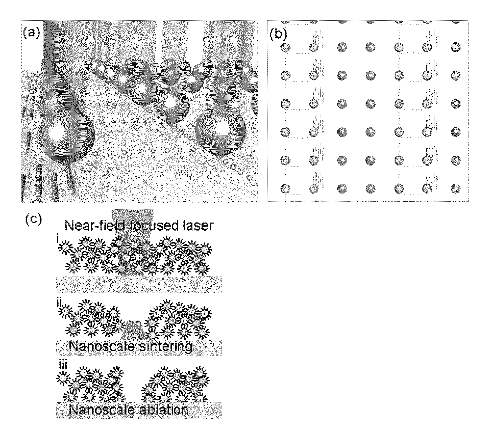
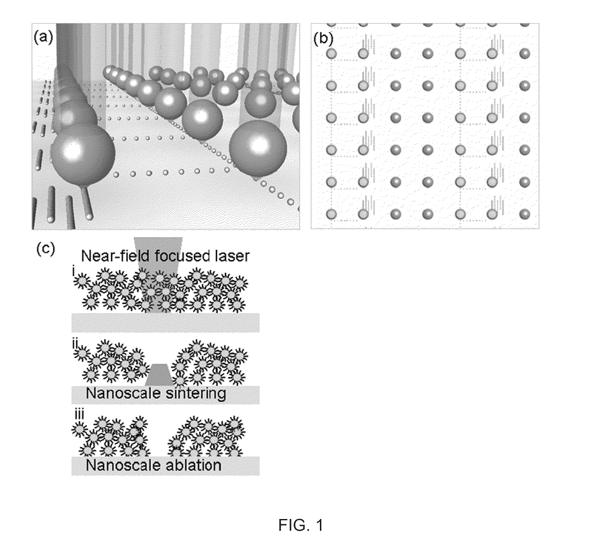
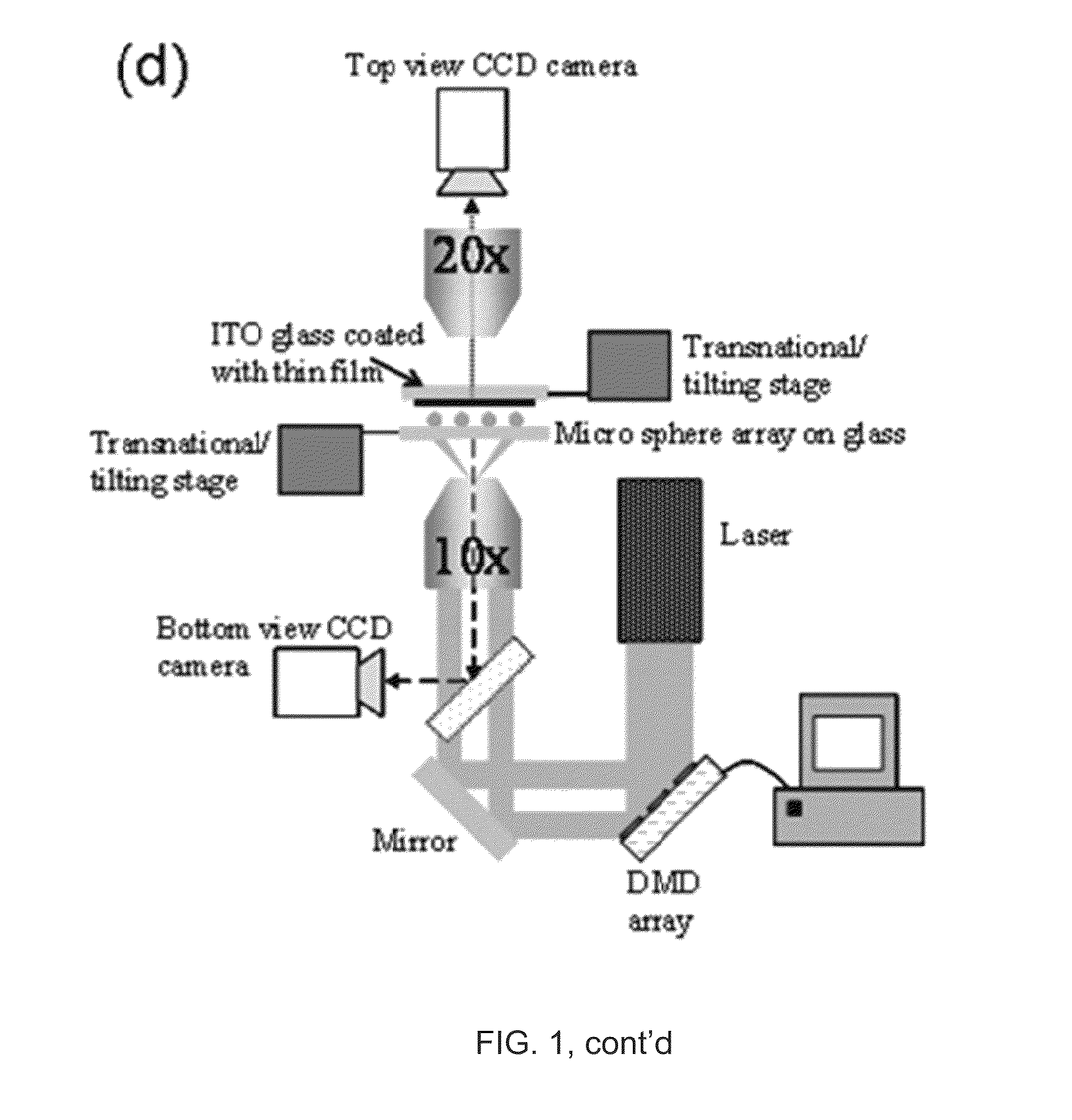
[0027]Methods of producing a nanostructure in a target film are provided. The method includes selectively irradiating at least one focusing element of a near-field focusing array that is in near-field focusing relationship with a target film in a manner sufficient to produce a nanostructure from the target film. Also provided are systems for practicing methods of the invention, as well as objects produced thereby.

[0028]Before the present invention is described in greater detail, it is to be understood that this invention is not limited to particular embodiments described, as such may, of course, vary. It is also to be understood that the terminology used herein is for the purpose of describing particular embodiments only, and is not intended to be limiting, since the scope of the present invention will be limited only by the appended claims.

[0029]Where a range of values is provided, it is understood that each intervening value, to the tenth of the unit of the lower limit unless the ...


PUM


Abstract

Methods of producing a nanostructure in a target film are provided. The method includes selectively irradiating at least one focusing element of a near-field focusing array that is in near-field focusing relationship with a target film in a manner sufficient to produce a nanostructure from the target film. Also provided are systems for practicing methods of the invention, as well as objects produced thereby.

Description

CROSS-REFERENCE TO RELATED APPLICATIONS[0001]Pursuant to 35 U.S.C. §119 (e), this application claims priority to the filing dates of: U.S. Provisional Patent Application Ser. No. 61 / 352,694 filed on Jun. 8, 2010; the disclosure of which application is herein incorporated by reference.GOVERNMENT RIGHTS[0002]This invention was made with government support under grant no. CMMI-0727841 awarded by National Science Foundation and grant no. N66001-08-1-2041 awarded by DARPA. The government has certain rights in the invention.INTRODUCTION[0003]Nanomanufacturing of nanoscale devices and patterns for various applications including nanobiosensing, displays and data storage, is an area of intense research. Essentially, it requires the generation of nanostructures of metals, semiconductors, metal oxides, polymers and biologically active molecules with well-defined feature size, shape, spacing, orientation and properties. In addition, the ability to masklessly generate arbitrary nanostructures of...

Claims


Application Information

Patent Timeline
IPC IPC(8): G03F7/20G03B27/00B82Y30/00
CPCB82Y30/00G03F7/70325G03F1/50B82Y40/00
Inventor HWANG, DAVID JENGRIGOROPOULOS, COSTAS P.
Owner RGT UNIV OF CALIFORNIA
Why Eureka
Try Eureka