Corrosion-resistant copper-to-aluminum bonds

a technology of copper-to-aluminum bonding and corrosion resistance, which is applied in the direction of semiconductor devices, semiconductor/solid-state device details, electrical apparatus, etc., can solve the problems of no grounded pin, no mal-functioning unit, and no cracking of the ball/pad interface, etc., to achieve easy implementation, high electrode potential, and easy supply by vendors

Inactive Publication Date: 2012-01-05
TEXAS INSTR INC
View PDF1 Cites 80 Cited by
  • Summary
  • Abstract
  • Description
  • Claims
  • Application Information

AI Technical Summary

Benefits of technology

[0009]Applicants solved the problem of copper oxidation by protecting the copper ball, when a thin layer (about 20 to 50 nm) of copper alloy enriched with a noble metal such as gold and palladium is enabled to grow in-situ on the copper side of the interface with the intermetallic layer. This in-situ accumulation can be realized by adding a small amount (for instance 0.5 to 5.0 weight %) of gold or palladium into the copper wire. After the doped copper ball, formed on the doped copper wire, is pressed onto the aluminum pad, a thin layer (about 50 to 100 nm) of copper / aluminum intermetallics will form at the interface as usual. For this formation of the intermetallic layer, copper atoms are taken into the intermetallic layer, leaving the noble atoms (either gold or palladium) behind. The more intermetallic compounds form (to a thickness of about 1.0 to 1.5 μm after HAST), the more atoms of gold pr palladium will be accumulated at the interface as a layer (about 100 to 200 nm thick) of Au- or Pd-enriched copper alloy on the copper ball. This alloy layer has a higher electrode potential and will act as a protective coating for the copper ball against electrochemical attack.
[0010]It is a technical advantage that copper wires doped with small amounts of gold or palladium can readily be supplied by vendors and can easily be implemented, because no new equipment for bonding is required and no change of the assembly flow process is needed.
[0011]It is another technical advantage that the high reliability of copper-bonded semiconductor devices by implementing the invention opens a wide window for selecting suitable molding compounds, packaging processes, device designs, and cost reduction.

Problems solved by technology

All mal-functioning units failed by cracking through the interface between the copper ball and the aluminum pad.
Applicants micro-analyzed the failed units and found first of all that the cracking of the ball / pad interface occurred only in the positively biased device pins, but not in any of the grounded pins.
Secondly, the layers of copper / aluminum intermetallic compounds between the aluminum pads and the copper balls were intact.
Applicants concluded that the root cause for the failure was the electrochemical corrosion of copper and the formation of a corrosion layer in the presence of high voltage and moisture.

Method used


Image

  • Corrosion-resistant copper-to-aluminum bonds
  • Corrosion-resistant copper-to-aluminum bonds
  • Corrosion-resistant copper-to-aluminum bonds

Examples


Embodiment Construction

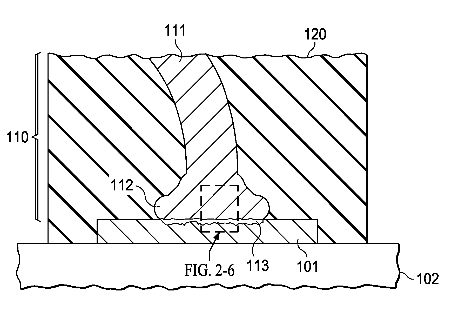
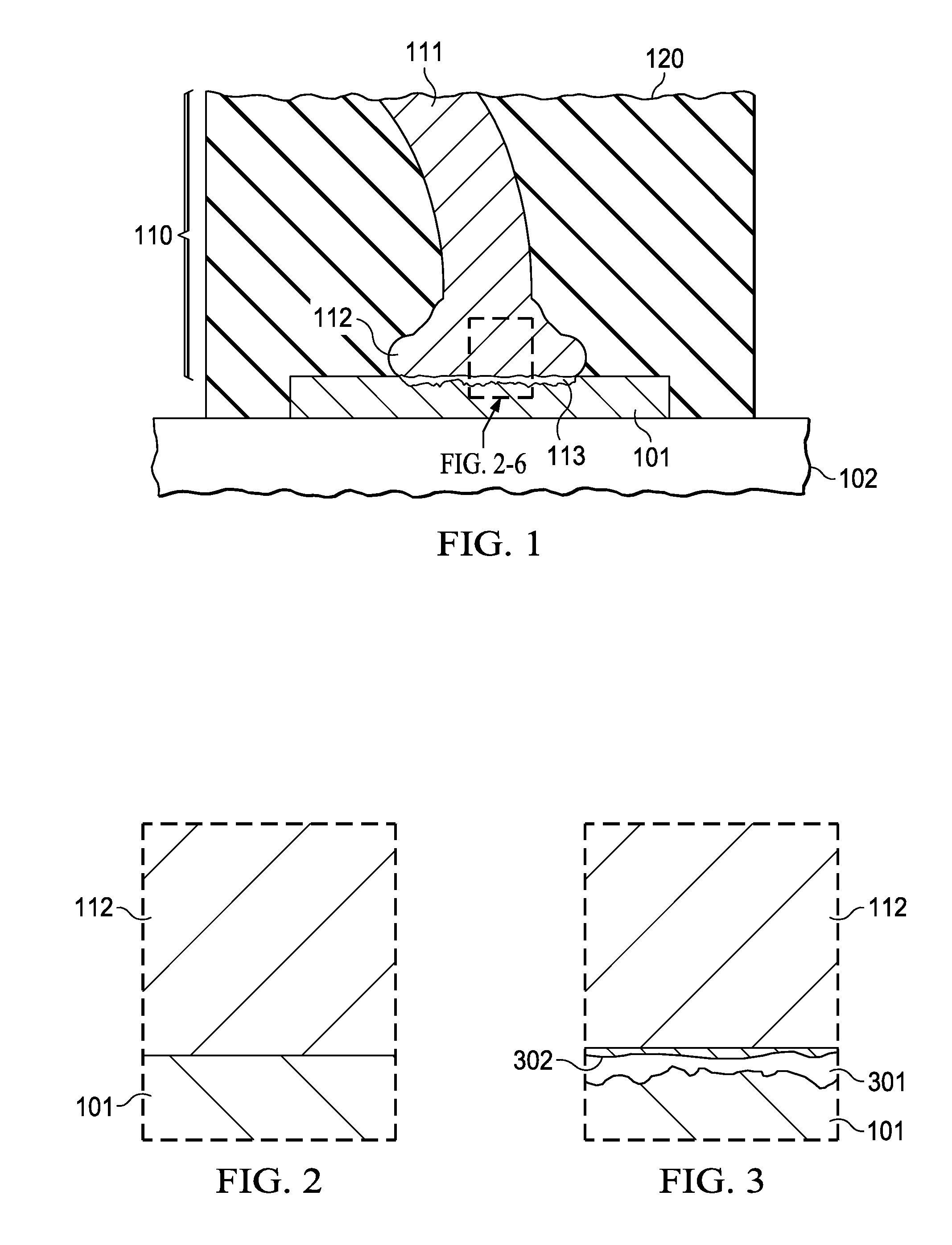
[0018]FIG. 1 displays schematically a terminal pad 101 of a semiconductor chip 102 contacted by a connecting wire 110. Terminal pad 101 is made of aluminum, often alloyed with 0.5 to 2% copper and / or 0.5 to 1% silicon. The pad is about 0.4 to 1.5 μm thick. Under the aluminum (not shown in FIG. 1) is frequently a thin layer (4 to 20 nm thick) of titanium, titanium nitride, titanium tungsten, tantalum, tantalum nitride, tantalum silicon nitride, tungsten nitride, or tungsten silicon nitride.

[0019]In FIG. 1, the connecting wire 110 includes a portion 111 of the round wire with a first diameter between about 15 to 33 μm, preferably 20 to 25 μm, and an end portion with a second diameter greater than the first diameter. Due to its shape, the end portion is often referred to as the wire nail head or the squashed wire sphere or ball. The wire consists of copper with an alloyed admixture of a noble metal such as gold or palladium. Alternative alloy options include the noble metals platinum a...


PUM

PropertyMeasurementUnit
thicknessaaaaaaaaaa
thickaaaaaaaaaa
thickaaaaaaaaaa

Abstract

A connection formed by a copper wire (112) alloyed with a noble metal in a first concentration bonded to a terminal pad (101) of a semiconductor chip; the end of the wire being covered with a zone (302) including an alloy of copper and the noble metal in a second concentration higher than the first concentration. When the noble metal is gold, the first concentration may range from about 0.5 to 2.0 weight %, and the second concentration from about 1.0 to 5.0 weight %. The zone of the alloy of the second concentration may have a thickness from about 20 to 50 nm.

Description

FIELD OF THE INVENTION[0001]The present invention is related in general to the field of metallurgical systems with application to electronic systems and semiconductor devices, and more specifically to the structure of semiconductor devices with aluminum-metallized contact pads contacted by ball bonds made from doped copper wires, and the reliability of these contacts under accelerated stress tests.DESCRIPTION OF RELATED ART[0002]Among the standardized reliability test of electronic devices are a group of tests, which investigate the sensitivity of wire-bonded and packaged semiconductor devices to moisture. In these tests, statistical amounts of wire bonds are tested in moisture-free (dry) ambient and compared to statistical amounts of wire bonds in moist ambient. The moisture tests look for failures caused by corroded metals, weakened contacts, leakage and delamination of device packages, and degraded electrical characteristics under functional operation.[0003]In the so-called THB t...

Claims


Application Information

Patent Timeline
Patent Type & Authority Applications(United States)
IPC IPC(8): H01L23/48
CPCH01L24/05H01L2924/01006H01L2224/05556H01L2224/05624H01L2224/45015H01L2224/45147H01L2224/48453H01L2224/48463H01L2224/48824H01L2924/01013H01L2924/01014H01L2924/01029H01L2924/0103H01L2924/01046H01L2924/01047H01L2924/0105H01L2924/01057H01L2924/01059H01L2924/01073H01L2924/01078H01L2924/01079H01L2924/01327H01L2924/20751H01L2924/20752H01L2924/20753H01L24/45H01L2924/01023H01L2924/01033H01L2224/04042H01L2224/48624H01L2224/45144H01L2924/01074H01L2924/00014H01L2924/00H01L2924/00015H01L2924/013H01L24/48H01L24/85H01L2924/00011H01L2924/181H01L2224/43848
Inventor ZENG, KEJUNPENG, WEI QUN
Owner TEXAS INSTR INC
Why Eureka
Try Eureka