Chip scale package and fabrication method thereof

Inactive Publication Date: 2012-01-19
SILICONWARE PRECISION IND CO LTD
View PDF6 Cites 6 Cited by
  • Summary
  • Abstract
  • Description
  • Claims
  • Application Information

AI Technical Summary

Benefits of technology

[0019]Therefore, the present invention mainly involves forming a protection layer on the active surface of a chip and fixing the inactive surface of the chip to a transparent hard carrier, then performing a molding process and removing the protection layer, and subsequently performing an RDL process so as to avoid the conventional problems caused by directly attaching the active surface of the chip on an adhesive film in the prior art, such as film-softening caused by heat, encapsulant overflow, chip deviation and contamination that lead to poor electrical connection between the wiring layer formed in a subsequent RDL process and the chip electrode pads and even waste product as a

Problems solved by technology

However, the application of the RDL technique or disposing of conductive traces on the chip is limited by the size of the chip or the area of the active surface of the chip.
Particularly, as chips are developed towards high integration and compact size, they do not have enough surface area for mounting of more solder balls for electrical connection to an external device.
However, since the chip is fixed by being attached to the adhesive film, deviation of the chip can easily occur due to film-softening and extension caused by heat, especially in the package molding process, thus adversely affecting the electrical connection between the electrode pads of the chip and the wring layer during the subsequent RDL process.
Further, the use of the adhesive film leads to

Method used


Image

  • Chip scale package and fabrication method thereof
  • Chip scale package and fabrication method thereof
  • Chip scale package and fabrication method thereof

Examples


Embodiment Construction

[0028]The following illustrative embodiments are provided to illustrate the disclosure of the present invention, these and other advantages and effects can be apparent to those in the art after reading this specification.

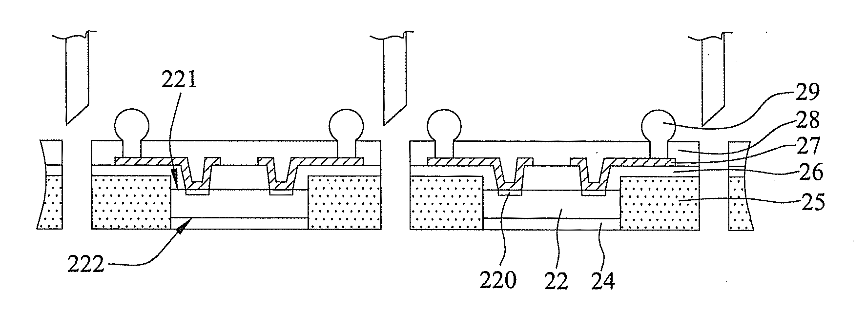
[0029]FIGS. 4A to 4H are cross-sectional views showing a chip scale package and a fabrication method thereof according to a first embodiment of the present invention.

[0030]Referring to FIGS. 4A and 4B, a wafer 22A having a plurality of chips 22 is provided, wherein the wafer 22A and the chips 22 each have an active surface 221 and an opposite inactive surface 222, and each of the chips 22 has a plurality of electrode pads 220 disposed on the active surface 221 thereof. Further, a protection layer 21 is formed on the active surface 221 of the wafer and has a thickness of about 3 to 20 μm. Then, the wafer 22A is cut into the plurality of chips 22 with the protection layer disposed on the active surface 221 thereof.

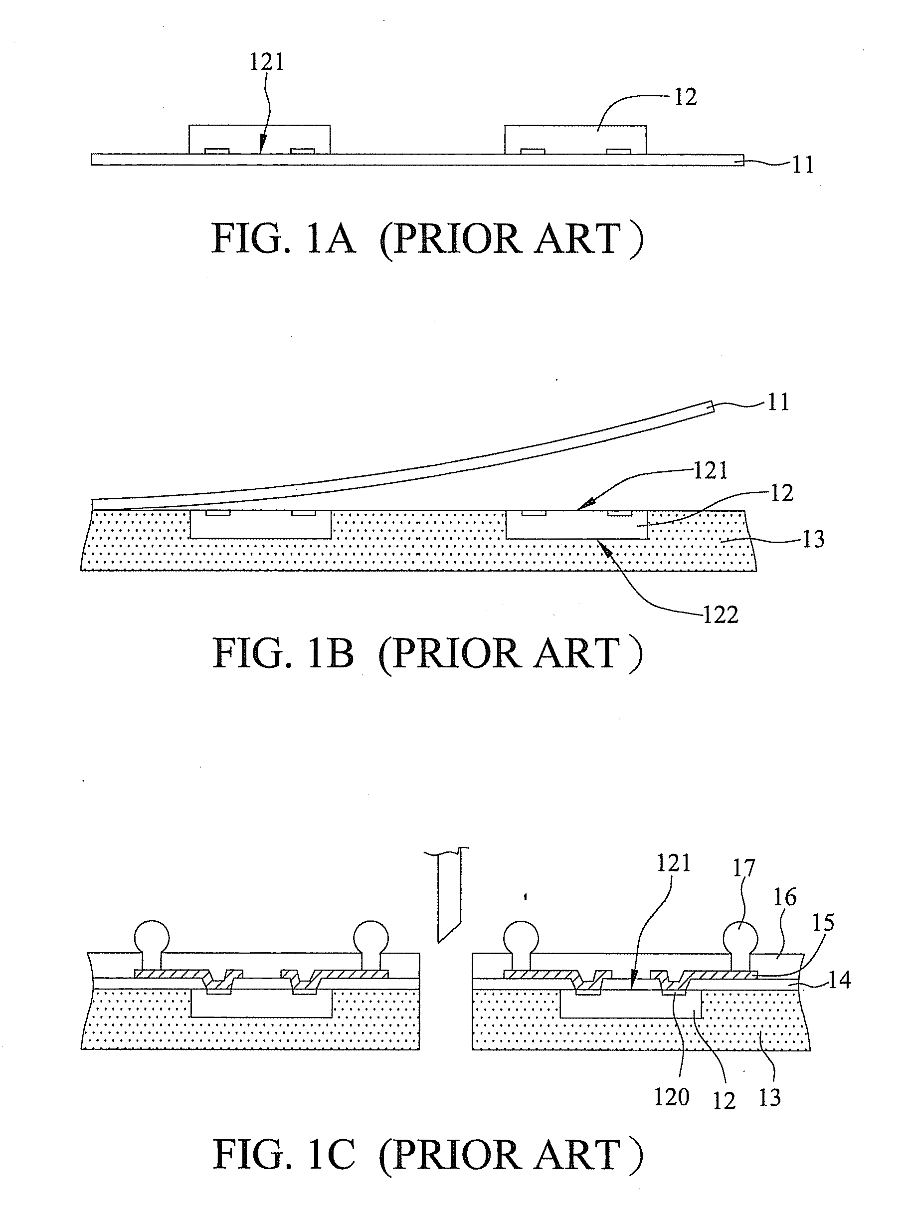
[0031]Referring to FIG. 4C, a transparent hard carrier...


PUM


Abstract

A fabrication method of a chip scale package is provided, which includes forming a protection layer on the active surface of a chip and fixing the inactive surface of the chip to a transparent carrier; performing a molding process; removing the protection layer from the chip and performing a redistribution layer (RDL) process, thereby solving the conventional problems caused by directly attaching the chip on an adhesive film, such as film-softening caused by heat, encapsulant overflow, warpage, chip deviation and contamination that lead to poor electrical connection between the wiring layer formed in the RDL process and the chip electrode pads and even waste product as a result. Further, the transparent carrier employed in the invention can be separated by laser and repetitively used in the process to help reduce the fabrication cost.

Description

BACKGROUND OF THE INVENTION[0001]1. Field of the Invention[0002]The present invention relates generally to semiconductor packages and fabrication methods thereof, and more particularly, to a chip scale package and a fabrication method thereof.[0003]2. Description of Related Art[0004]A chip scale package (CSP) is characterized in that the package size is equivalent to the size of the chip that is disposed in the package. U.S. Pat. No. 5,892,179, No. 6,103,552, No. 6,287,893, No. 6,350,668 and No. 6,433,427 disclose a conventional CSP structure, wherein a built-up structure is directly formed on a chip without using a chip carrier, such as a substrate or a lead frame, and a redistribution layer (RDL) technique is used to accomplish a redistribution of the electrode pads of the chip to a desired pattern.[0005]However, the application of the RDL technique or disposing of conductive traces on the chip is limited by the size of the chip or the area of the active surface of the chip. Parti...

Claims


Application Information

Patent Timeline
IPC IPC(8): H01L23/485H01L21/786
CPCH01L21/561H01L2224/0401H01L24/19H01L24/96H01L2221/68359H01L2224/04105H01L2224/20H01L2224/96H01L2924/01082H01L2924/18162H01L23/3121H01L2224/12105H01L2924/01033H01L2924/014H01L2224/82H01L2924/3511H01L2924/00
Inventor CHANG, CHIANG-CHENGHUANG, CHIEN-PINGKE, CHUN-CHI
Owner SILICONWARE PRECISION IND CO LTD
Why Eureka
Try Eureka