Semiconductor device

Inactive Publication Date: 2012-01-19
SEMICON ENERGY LAB CO LTD
View PDF6 Cites 19 Cited by
  • Summary
  • Abstract
  • Description
  • Claims
  • Application Information

AI Technical Summary

Benefits of technology

[0024]In addition, in one embodiment of the disclosed invention, a bit line is divided through selection transistors in each block of a memory cell array

Problems solved by technology

A transistor formed using a highly-purified oxide semiconductor can reta

Method used


Image

  • Semiconductor device
  • Semiconductor device
  • Semiconductor device

Examples


Example

Embodiment 1

[0042]In this embodiment, circuit structures and operation of semiconductor devices in one embodiment of the disclosed invention are described with reference to FIGS. 1A-1 and 1A-2, FIG. 2, FIG. 3, and FIG. 4. Note that in some circuit diagrams, “OS” is written beside a transistor in order to indicate that the transistor includes an oxide semiconductor.

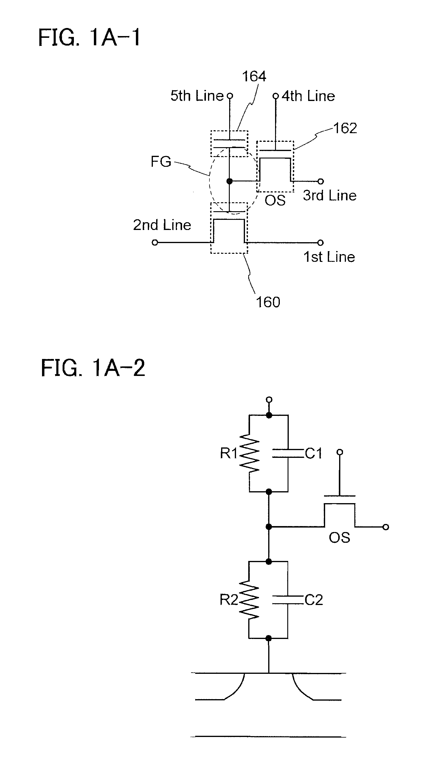
[0043]First, a basic circuit structure and operation of the circuit are described with reference to FIGS. 1A-1 and 1A-2. In the semiconductor device illustrated in FIG. 1A-1, a first wiring (1st Line) and a source electrode of a transistor 160 are electrically connected to each other, and a second wiring (2nd Line) and a drain electrode of the transistor 160 are electrically connected to each other. In addition, a third wiring (3rd Line) and a source electrode (or a drain electrode) of a transistor 162 are electrically connected to each other, and a fourth wiring (4th Line) and a gate electrode of the transistor 162 are el...

Example

Application Example 1

[0068]Next, a more specific circuit structure to which the circuit illustrated in FIGS. 1A-1 and 1A-2 is applied and operation of the circuit are described with reference to FIG. 2, FIG. 3, and FIG. 4.

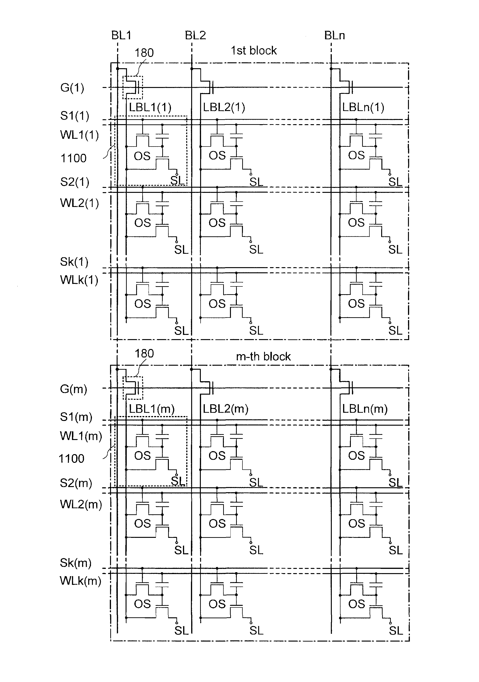
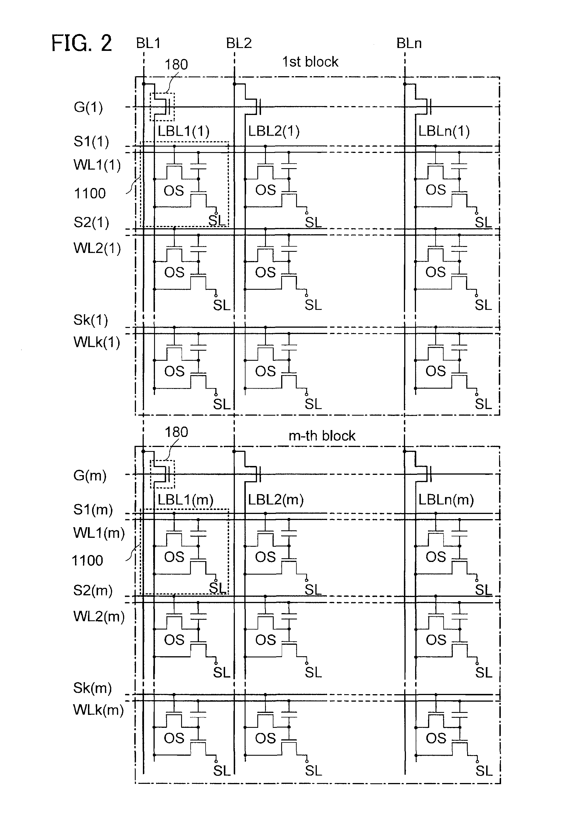
[0069]FIG. 2 is an example of a circuit diagram of a semiconductor device including a plurality of memory cells that are divided into blocks every plural rows. In the semiconductor device of one embodiment of the present invention, a memory cell 1100 includes memory cell arrays that are divided into m blocks (a first block to an m-th block, where m is an integer of 2 or more) every k rows (k is an integer of 2 or more) and are arranged in matrix of k×m columns in the vertical direction by n rows (n is an integer of 2 or more) in the horizontal direction; k×m signal lines S; k×m word lines WL; n common bit lines BL; a common source line SL used in common among the memory cells; m selection lines G; m×n selection transistors 180; and m×n divided bit lines LBL. Note t...

Example

Embodiment 2

[0107]In this embodiment, a structure and a method for manufacturing a semiconductor device of one embodiment of the disclosed invention are described with reference to FIGS. 5A and 5B, FIGS. 6A and 6B, FIGS. 7A to 7E, FIGS. 8A to 8C, FIGS. 9A to 9D, and FIGS. 10A to 10C.

[0108]FIGS. 5A and 5B illustrate an example of the structure of a semiconductor device corresponding to the circuit illustrated in FIG. 1A-1 or the memory cell 1100 illustrated in FIG. 2. FIG. 5A is a cross-sectional view of the semiconductor device, and FIG. 5B is a plan view of the semiconductor device. Here, FIG. 5A corresponds to a cross section taken along line A1-A2 and line B1-B2 in FIG. 5B. Note that in FIG. 5B, some of components of the semiconductor device (e.g., wirings 154 and 158) are omitted in order to avoid complexity.

[0109]The semiconductor device illustrated in FIGS. 5A and 5B includes the transistor 160 including a first semiconductor material in a lower portion and the transistor 162 ...


PUM


Abstract

A plurality of memory cells included in a memory cell array are divided into a plurality of blocks every plural rows. A common bit line is electrically connected to the divided bit lines through selection transistors in the blocks. One of the memory cells includes a first transistor, a second transistor, and a capacitor. The first transistor includes a first channel formation region. The second transistor includes a second channel formation region. The first channel formation region includes a semiconductor material different from the semiconductor material of the second channel formation region.

Description

TECHNICAL FIELD[0001]The disclosed invention relates to semiconductor devices including semiconductor elements and methods for manufacturing the semiconductor devices.BACKGROUND ART[0002]Memory devices including semiconductor elements are broadly classified into two categories: volatile memory devices that lose stored data when power is not supplied and non-volatile memory devices that retains stored data even when power is not supplied.[0003]A typical example of a volatile memory device is a DRAM (dynamic random access memory). A DRAM stores data in such a manner that a transistor included in a memory element is selected and electrical charge is accumulated in a capacitor.[0004]When data is read from a DRAM, electrical charge in a capacitor is lost according to the principle; thus, another writing operation is necessary every time data is read. Further, a transistor included in a memory element has leakage current (off-state current) between a source and a drain in an off state or ...

Claims


Application Information

Patent Timeline
IPC IPC(8): G11C5/06
CPCG11C11/404H01L27/1207H01L27/1156G11C16/0441H10B41/70H10B41/35
Inventor KATO, KIYOSHIMATSUZAKI, TAKANORIINOUE, HIROKINAGATSUKA, SHUHEI
Owner SEMICON ENERGY LAB CO LTD
Why Eureka
Try Eureka