Iii-nitride light-emitting diode and method of producing the same

a technology of light-emitting diodes and nitride, which is applied in the direction of semiconductor/solid-state device manufacturing, electrical apparatus, semiconductor devices, etc., can solve the problems of dramatic drop in the efficiency of ingan emission, efficiency and light quality of phosphor-convertible devices, and still imperfect, etc., to achieve simple, economical, efficient method, and improve performance and properties

Active Publication Date: 2012-02-02
NATIONAL TSING HUA UNIVERSITY
View PDF1 Cites 17 Cited by
  • Summary
  • Abstract
  • Description
  • Claims
  • Application Information

AI Technical Summary

Benefits of technology

[0006]An object of the present invention is to provide light-emitting diodes having better performance and properties than prior art. In addition, the green-yellow-gap and efficiency droop issue can be overcome. Moreover, a simple, economical, efficient method to produce such light-emitting diodes is also needed.
[0017]In one embodiment, the first electrode or the second electrode is a transparent electrode, and each of the p-type GaN nanorods or n-type GaN nanorods near the transparent electrode has two ends wherein one end near the transparent electrode is wider than the other end, forming a continuously connected nanorod network without significant current leakage.

Problems solved by technology

However, this potential is limited by the dramatic drop in the InGaN emission efficiency at longer wavelengths2-5.
The efficiency and light quality of phosphor-converted devices, however, are still imperfect due to the Stokes shift loss and limited color rendering1,2.
Therefore, growth of high-In-content InGaN / GaN quantum wells would unavoidably result in a high density of defects and huge internal electrostatic (piezoelectric) fields (>1 MV / cm)6,7.
The internal fields in the InGaN wells spatially separate the electron and hole wave functions, i.e., quantum confined Stark effect (QCSE), making highly efficient longer-wavelength LEDs difficult to achieve based on polar c-plane structures.
Unfortunately, these are not applicable in the case of high-In-content InGaN quantum wells because of the lack of strong charge localization and increasingly large internal electrostatic fields.
Besides, there are other QCSE- and ultrathin-well-related detrimental features of c-plane InGaN LEDs, including efficiency droop and blue-shift of the emission wavelength (due to carrier screening of internal electrostatic fields) with increasing drive current.
However, the nonpolar approach has its own limitations and challenges8 such that ideal solutions for the green-yellow-gap and efficiency droop issues are still lacking.

Method used


Image

  • Iii-nitride light-emitting diode and method of producing the same
  • Iii-nitride light-emitting diode and method of producing the same
  • Iii-nitride light-emitting diode and method of producing the same

Examples


Embodiment Construction

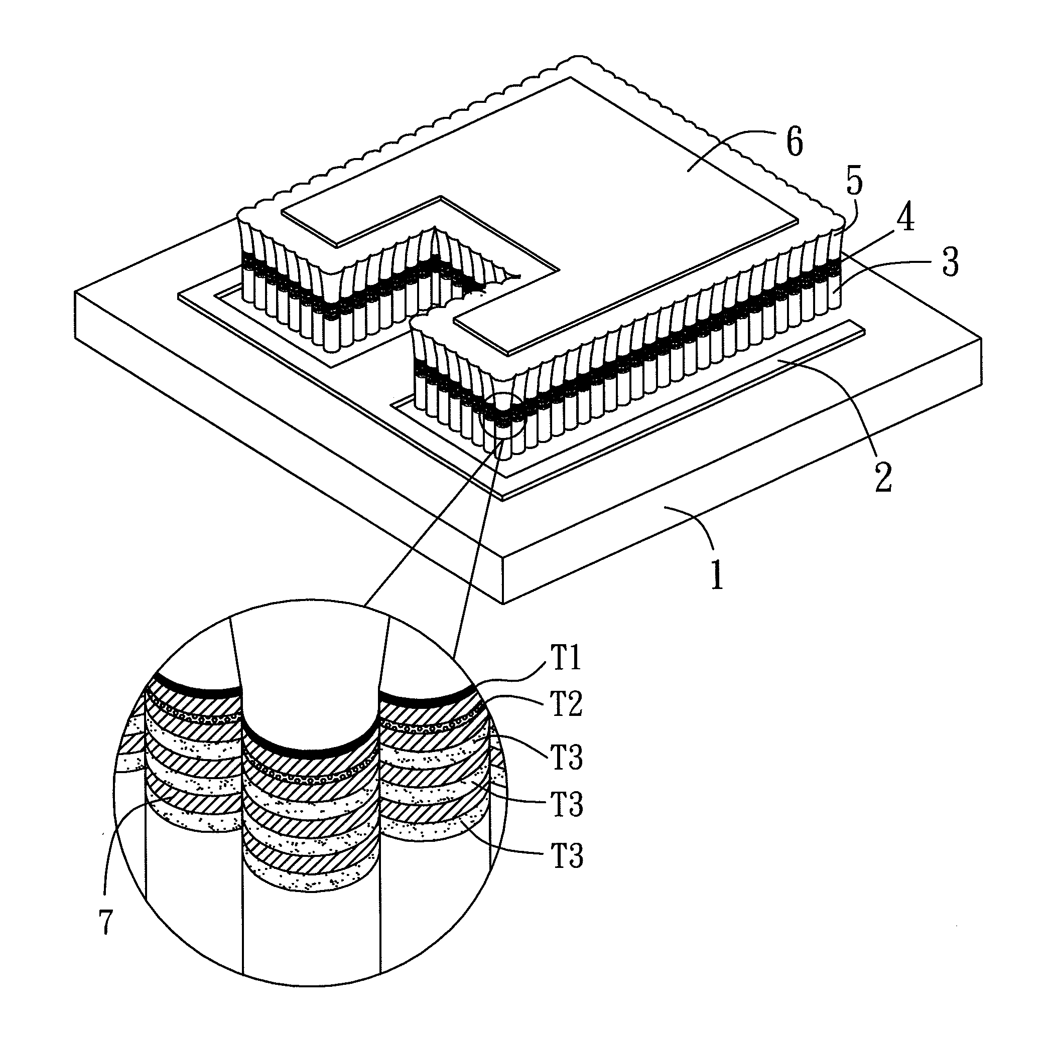
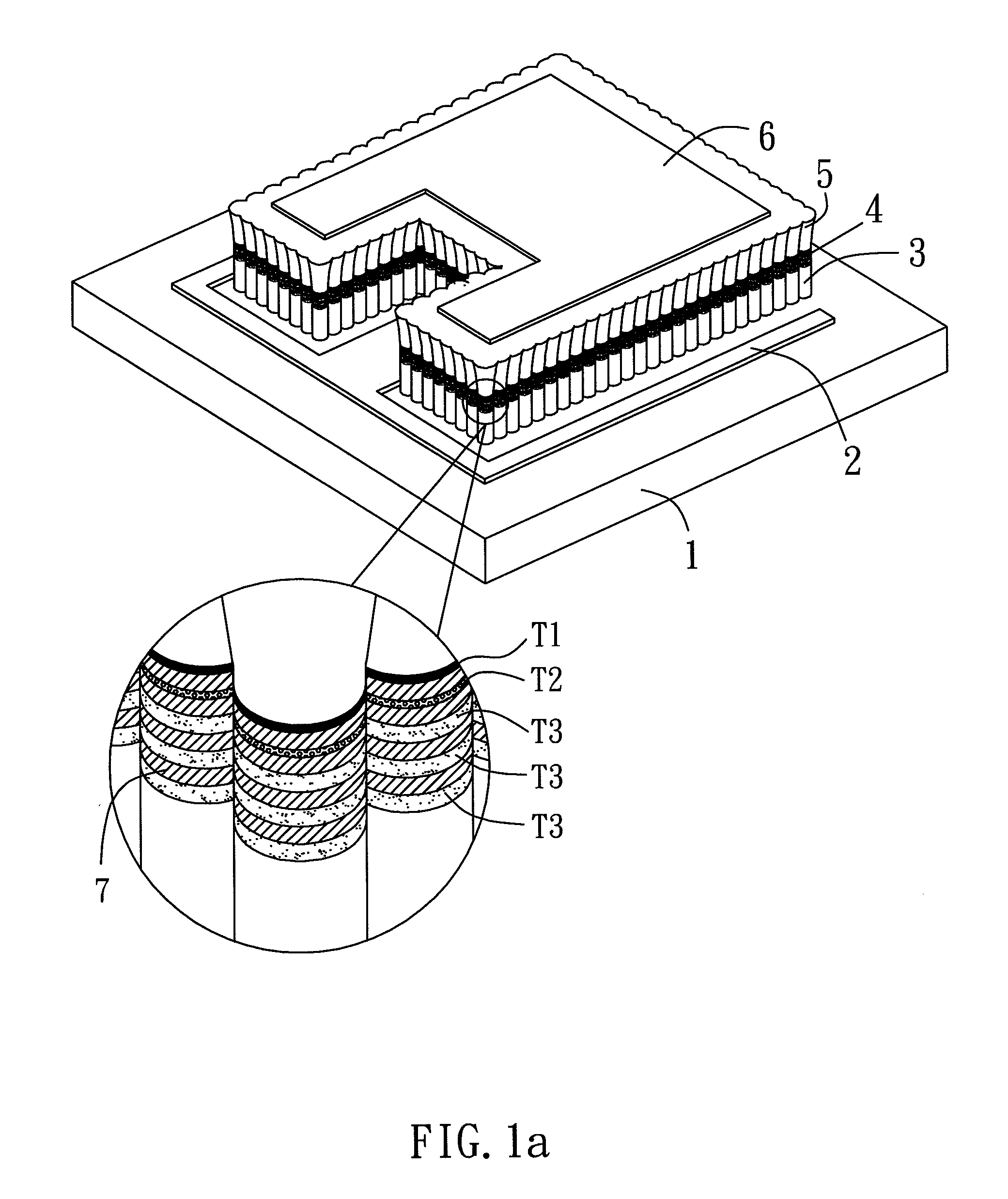
[0041]Reference will now be made in detail to specific embodiments of the invention. Examples of these embodiments are illustrated in accompanying drawings. While the invention will be described in conjunction with these specific embodiments, it will be understood that it is not intended to limit the invention to these embodiments. On the contrary, it is intended to cover alternatives, modifications, and equivalents as may be included within the spirit and scope of the invention as defined by the appended claims. In the following description, numerous specific details are set forth in order to provide a through understanding of the present invention. The present invention may be practiced without some or all of these specific details. In other instances, well-known process operations and components are not been described in detail in order not to unnecessarily obscure the present invention. While drawings are illustrated in details, it is appreciated that the quantity of the disclos...


PUM

PropertyMeasurementUnit
thicknessaaaaaaaaaa
thicknessaaaaaaaaaa
color temperatureaaaaaaaaaa

Abstract

Embodiments of the present invention provides III-nitride light-emitting diodes, which primarily include a first electrode, a n-type gallium nitride (GaN) nanorod array consisted of one or more n-type GaN nanorods ohmic contacting with the first electrode, one or more indium gallium nitride (InGaN) nanodisks disposed on each of the n-type GaN nanorods, a p-type GaN nanorod array consisted of one or more p-type GaN nanorods, where one p-type GaN nanorod is disposed on top of the one ore more InGaN nanodisks disposed on each of the n-type GaN nanorods, and a second electrode ohmic contacts with the p-type GaN nanorod array.

Description

FIELD OF THE INVENTION[0001]The present invention relates to III-nitride light-emitting diodes and their forming methods.DESCRIPTION OF THE PRIOR ART[0002]Solid-state light sources based on white light emitting diode (LED) technology have gained much attention because of their tremendous potential for energy-efficient general illumination applications. In white LEDs, the luminous efficacy and color rendering can be controlled by light mixing of polychromatic (e.g., red, yellow, green, blue) emitters1,2. At present, the indium gallium nitride (InGaN) compound semiconductor alloys are considered as the most promising material system for white LEDs since the direct band gaps of InxGa1−xN (0≦x≦1) can be continuously tuned from the near-infrared (0.6 eV, InN) to near-UV (3.4 eV, GaN) region, including the entire visible spectrum. However, this potential is limited by the dramatic drop in the InGaN emission efficiency at longer wavelengths2-5. To date, efficient InGaN LEDs are only availa...

Claims


Application Information

Patent Timeline
Patent Type & Authority Applications(United States)
IPC IPC(8): H01L33/30H01L33/00
CPCH01L33/007H01L33/08H01L33/38H01L33/20H01L33/18H01L33/30
Inventor GWO, SHANG-JRLIN, HON-WAYLU, YU-JUNG
Owner NATIONAL TSING HUA UNIVERSITY
Why Eureka
Try Eureka