Semiconductor device

a semiconductor and transistor technology, applied in the direction of semiconductor devices, basic electric elements, electrical equipment, etc., can solve the problems of delay in the practical use of oxide semiconductors, and achieve the effect of stable electrical characteristics

Inactive Publication Date: 2012-02-23
SEMICON ENERGY LAB CO LTD
View PDF1 Cites 31 Cited by
  • Summary
  • Abstract
  • Description
  • Claims
  • Application Information

AI Technical Summary

Benefits of technology

[0018]According to one embodiment of the present invention, it is possible to provide a transistor which hardly deteriorates owing to light irradiation and has stable electrical characteristics and a semiconductor device including the transistor.

Problems solved by technology

Any method for improving such a change in the characteristics caused by light in a transistor including an oxide semiconductor has not been proposed, which causes a delay in practical use of the oxide semiconductor which is expected as a new material.

Method used


Image

  • Semiconductor device
  • Semiconductor device
  • Semiconductor device

Examples


embodiment 1

[0055]In this embodiment, an example of a semiconductor device according to one embodiment of the present invention will be described with reference to FIGS. 6A to 6C, FIGS. 7A to 7C, FIGS. 8A to 8C, and FIGS. 9A to 9C.

[0056]FIGS. 6A to 6C are a plan view and cross-sectional views of a transistor 310 as an example of a semiconductor device according to one embodiment of the disclosed invention. In FIGS. 6A to 6C, a bottom-gate transistor is illustrated as a transistor according to one embodiment of the disclosed invention. Here, FIG. 6A is a plan view and FIGS. 6B and 6C are cross-sectional views taken along line A-B and line C-D, respectively, of FIG. 6A. Note that part of components of the transistor 310 (e.g., a protective insulating film 407 and the like) is omitted in FIG. 6A for brevity.

[0057]The transistor 310 in FIGS. 6A to 6C includes, over a substrate 400 having an insulating surface, a gate electrode 401, a gate insulating layer 402, an oxide semiconductor layer 409, a so...

embodiment 2

[0085]Hereinafter, an example of a manufacturing process of a transistor according to this embodiment will be described with reference to FIGS. 12A to 12E.

[0086]An example of a manufacturing process of the transistor 310 in FIGS. 6A to 6C will be described with reference to FIGS. 12A to 12E. Note that a material and a method (including an interchange of the order of steps) which are similar to those of the transistor 310 can be used for the cases of other transistors.

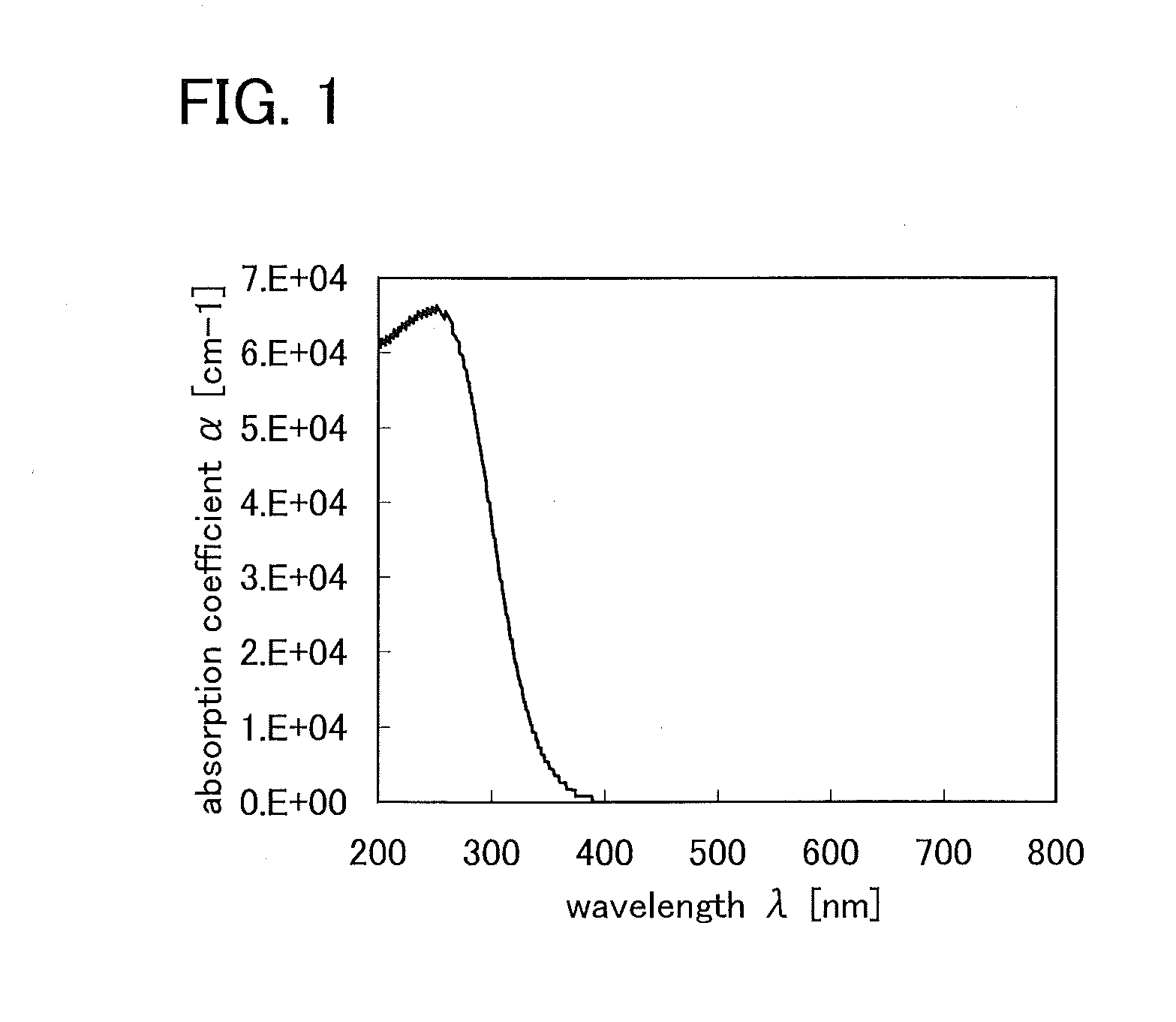
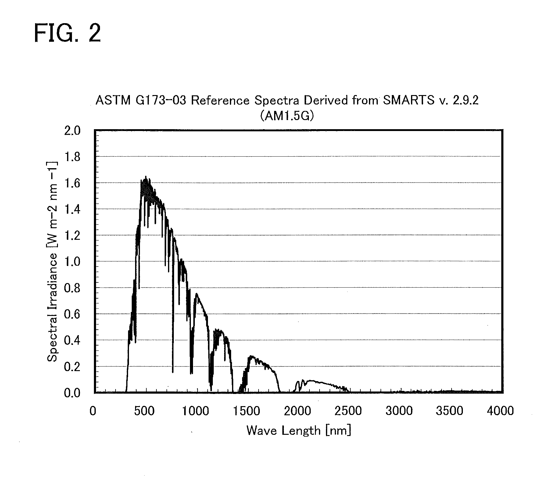
[0087]As for the thickness of each layer, the thickness of each layer in the portion corresponding to the light path when light enters the channel portion of the oxide semiconductor layer 409 is adjusted to a prescribed thickness described in one embodiment of the present invention. In consideration of the refractive index of each layer, the thickness in deposition is adjusted as appropriate so that the finished thickness is the prescribed thickness.

[0088]First, a conductive film is formed over the substrate 400 having ...

embodiment 3

[0154]A semiconductor device (also referred to as a display device) with a display function can be manufactured using any of the transistors exemplified in Embodiment 1 and Embodiment 2. Moreover, some or all of the driver circuits which include the transistors can be formed over a substrate where the pixel portion is formed, whereby a system-on-panel can be obtained.

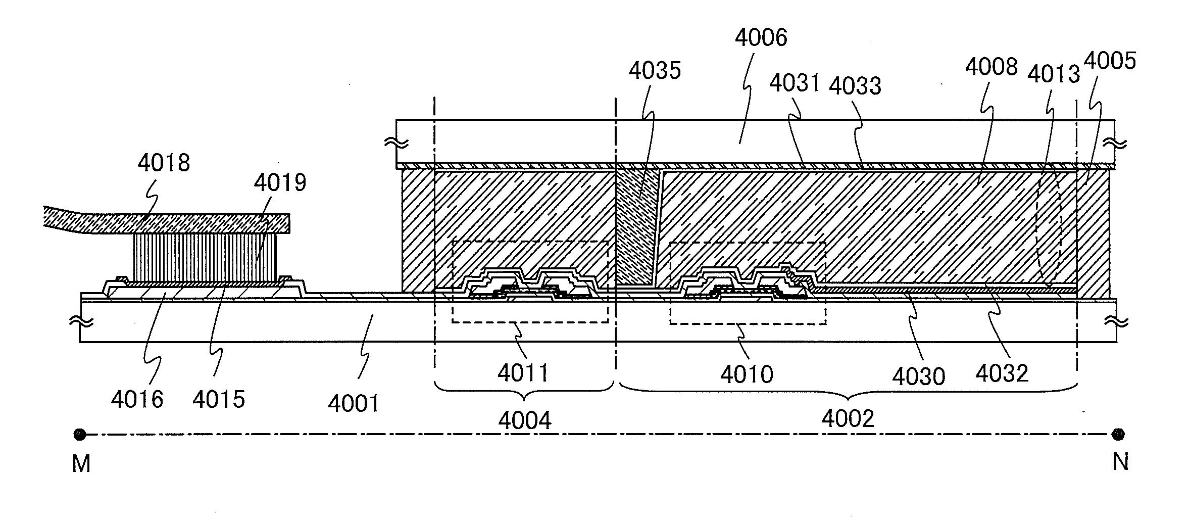
[0155]In FIG. 13A, a sealant 4005 is provided so as to surround a pixel portion 4002 provided over a first substrate 4001, and the pixel portion 4002 is sealed between the first substrate 4001 and a second substrate 4006. In FIG. 13A, a signal line driver circuit 4003 and a scan line driver circuit 4004 which are formed using a single crystal semiconductor film or a polycrystalline semiconductor film over a substrate separately prepared are mounted over the first substrate 4001, in a region that is different from the region surrounded by the sealant 4005. Various signals and potential are supplied to the signal line dri...


PUM


Abstract

An object is to provide a transistor in which light deterioration is suppressed as much as possible and electrical characteristics are stable, and a semiconductor device including the transistor. The attention focuses on the fact that light is reflected by a film used for forming a transistor and multiple interaction occurs. When the optical thickness of the film which causes the reflection is roughly an odd multiple of λ0/4 or roughly an even multiple of λ0/4, reflectance in a wavelength region of light which is absorbed by an oxide semiconductor is increased without a loss of a function of the film with respect to the transistor, whereby the amount of light absorbed by the oxide semiconductor is reduced and an effect of reducing light deterioration is increased.

Description

BACKGROUND OF THE INVENTION[0001]1. Field of the Invention[0002]The present invention relates to a transistor and a semiconductor device at least part of which includes the transistor.[0003]In this specification, a semiconductor device means all types of devices which can function by utilizing semiconductor characteristics, and an electro-optical device such as a liquid crystal display device, a semiconductor circuit, and an electronic device are all semiconductor devices.[0004]2. Description of the Related Art[0005]Although transistors including silicon semiconductors have been used for conventional display devices typified by liquid crystal televisions, oxide semiconductors have attracted attention as a material which replaces silicon semiconductors. For example, an active matrix display device, in which an amorphous oxide including indium (In), gallium (Ga), and zinc (Zn) is used for an active layer of a transistor and the electron carrier concentration of the amorphous oxide is ...

Claims


Application Information

Patent Timeline
Patent Type & Authority Applications(United States)
IPC IPC(8): H01L29/04
CPCH01L29/42384H01L29/78696H01L29/7869H01L29/78633H01L29/78648H01L27/1225
Inventor GODO, HIROMICHIMURAYAMA, KEISUKE
Owner SEMICON ENERGY LAB CO LTD
Why Eureka
Try Eureka