Sputtering target and method for manufacturing semiconductor device

a technology of semiconductor devices and target devices, which is applied in the direction of semiconductor devices, vacuum evaporation coatings, coatings, etc., can solve the problems of insufficient characteristics of a semiconductor element which is manufactured using oxide semiconductors, and achieve the effect of high reliability of semiconductor elements

Active Publication Date: 2012-03-08
SEMICON ENERGY LAB CO LTD
View PDF3 Cites 15 Cited by
  • Summary
  • Abstract
  • Description
  • Claims
  • Application Information

AI Technical Summary

Benefits of technology

[0018]In one embodiment of the present invention, a sputtering target containing a small amount of impurities such as a hydrogen atom, an alkali metal, and an alkaline earth metal can be provided. An oxide semiconductor film in ...

Problems solved by technology

However, characteristics of a semiconductor element which is...

Method used


Image

  • Sputtering target and method for manufacturing semiconductor device
  • Sputtering target and method for manufacturing semiconductor device
  • Sputtering target and method for manufacturing semiconductor device

Examples


embodiment 1

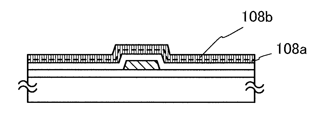
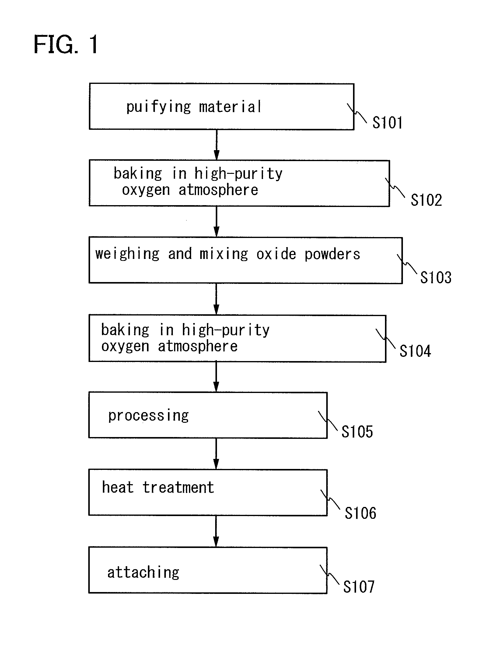
[0024]In this embodiment, a method for manufacturing a sputtering target which is one embodiment of the present invention will be described with reference to FIG. 1. FIG. 1 is a flow chart illustrating an example of a method for manufacturing a sputtering target according to this embodiment.

[0025]First, plural kinds of single metals (Zn, In, Al, Sn, and the like) that are materials of the sputtering target are each purified by repeating distillation, sublimation, or recrystallization (S101). After that, purified metals are each processed into a powder form. Note that in the case of using Ga or Si as the material of the sputtering target, a single crystal is obtained by a zone melt method or a Czochralski method and then processing into a powder form is performed. Then, each of the sputtering target materials is baked in a high-purity oxygen atmosphere so as to be oxidized (S102). Subsequently, each of the oxide powders is weighed as appropriate, and the weighed oxide powders are mix...


PUM

PropertyMeasurementUnit
Carrier concentrationaaaaaaaaaa

Abstract

An object is to provide a deposition technique for depositing an oxide semiconductor film. Another object is to provide a method for manufacturing a highly reliable semiconductor element using the oxide semiconductor film. A novel sputtering target obtained by removing an alkali metal, an alkaline earth metal, and hydrogen that are impurities in a sputtering target used for deposition is used, whereby an oxide semiconductor film containing a small amount of those impurities can be deposited.

Description

TECHNICAL FIELD[0001]The present invention relates to a sputtering target and a method for manufacturing the sputtering target. Further, the present invention relates to a method for manufacturing a semiconductor device which is manufactured with the use of the sputtering target and uses an oxide semiconductor.[0002]In this specification, a semiconductor device means a general device which can function by utilizing semiconductor characteristics, and an electro-optic device, a semiconductor circuit, and an electronic device are all semiconductor devices.BACKGROUND ART[0003]A transistor formed over a flat plate such as a glass substrate, which is typically used in a liquid crystal display device, is generally formed using a semiconductor material such as amorphous silicon or polycrystalline silicon. A transistor manufactured using amorphous silicon has low field effect mobility, but can be formed over a larger glass substrate. In contrast, a transistor manufactured using polycrystalli...

Claims


Application Information

Patent Timeline
IPC IPC(8): H01L29/227H01L21/363H01L29/24
CPCC23C14/086C23C14/3414H01L29/66742H01L21/02631H01L29/66969H01L21/02565H01L29/7869C23C14/34H01L21/34C23C14/081
Inventor YAMAZAKI, SHUNPEI
Owner SEMICON ENERGY LAB CO LTD
Why Eureka
Try Eureka