Light emitting diode package

Active Publication Date: 2012-03-08
SEOUL SEMICONDUCTOR
View PDF3 Cites 75 Cited by
  • Summary
  • Abstract
  • Description
  • Claims
  • Application Information

AI Technical Summary

Benefits of technology

[0033]According to one embodiment, the light emitting diode package may operate at high voltage and prevent an increase of a package size by adopting a light emitting diode chip having a plurality of light emitting cells connected in series. Further, it is possible to realize various colors by a combination of the light emitting diode chip having the light emitting cells connected in series and another light emitting diode chip emitting light having a different frequency from the light emitting diode chip. Further, these light emitting diode chips are mounted on landing pads separated from each other, thereby preventing current leakage from the light emitting diode chips. The landing pads dissipate heat from the light emitting diode chips, thereby enhancing heat dissipation of the light emitting diode package. In addition, it is possible to realize high output of white light, in particular, warm white light, under a high voltage by a combination of a blue light emitting diode chip, a plurality of red light emitting diode chips and a phosphor. Further, it is possible to prevent moisture infiltration from outside by a combination of a gel-type silicone molding portion, a high hardness silicone bonding agent, and a glass lens.
[0034]In another embodiment, the package body comprises a package lower part and a package upper part, and a middle layer comprising conductive patterns such as a landing pad(s) and a bonding pad(s) is interposed between the package upper part and the package lower part, in which at least some of the conducive patterns extend to a lower side of the package body along a side surface of the package body to be exposed to the outside, so that the light emitting diode package has improved heat dissipation. Furthermore, the conductive patterns fixedly surround the package lower part, in particular, two or more layers of dielectric subst

Problems solved by technology

However, since the white light emitting device composed of the combination of the blue light emitting diode and the yellow phosphor emits white light having high color temperature due to lack of a red color region, it is not suitable for regular lighting.
While a red phosphor may be also used to realize a warm white color having low color temperature, application of the red phosphor is limited due to low optical efficiency of the red phosphor.
Further, phosphors react with moisture absorbed from the outside and experience efficiency deterioration over time, thereby reducing operational lifespan of the light emitting device and, in particular, the red phosphor experiences more rapid efficiency deterioration than a green or yellow phosphor, thereby further reducin

Method used


Image

  • Light emitting diode package
  • Light emitting diode package
  • Light emitting diode package

Examples


first embodiment

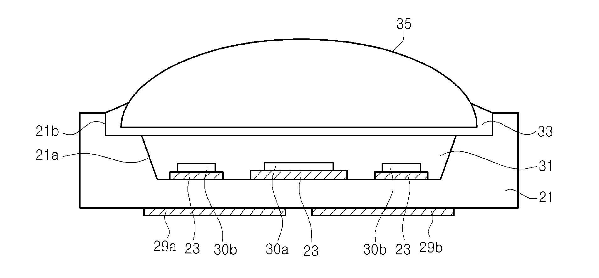
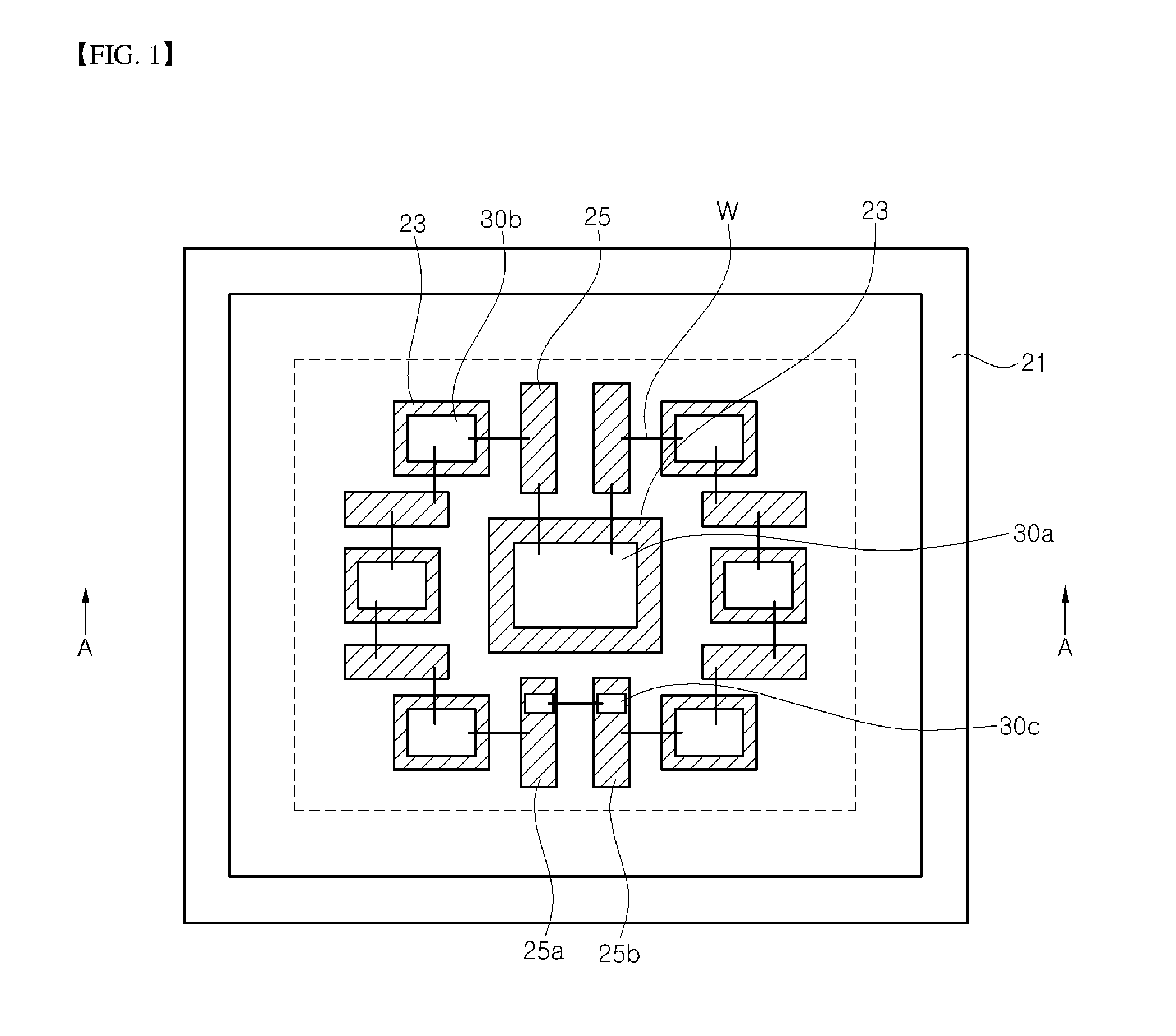
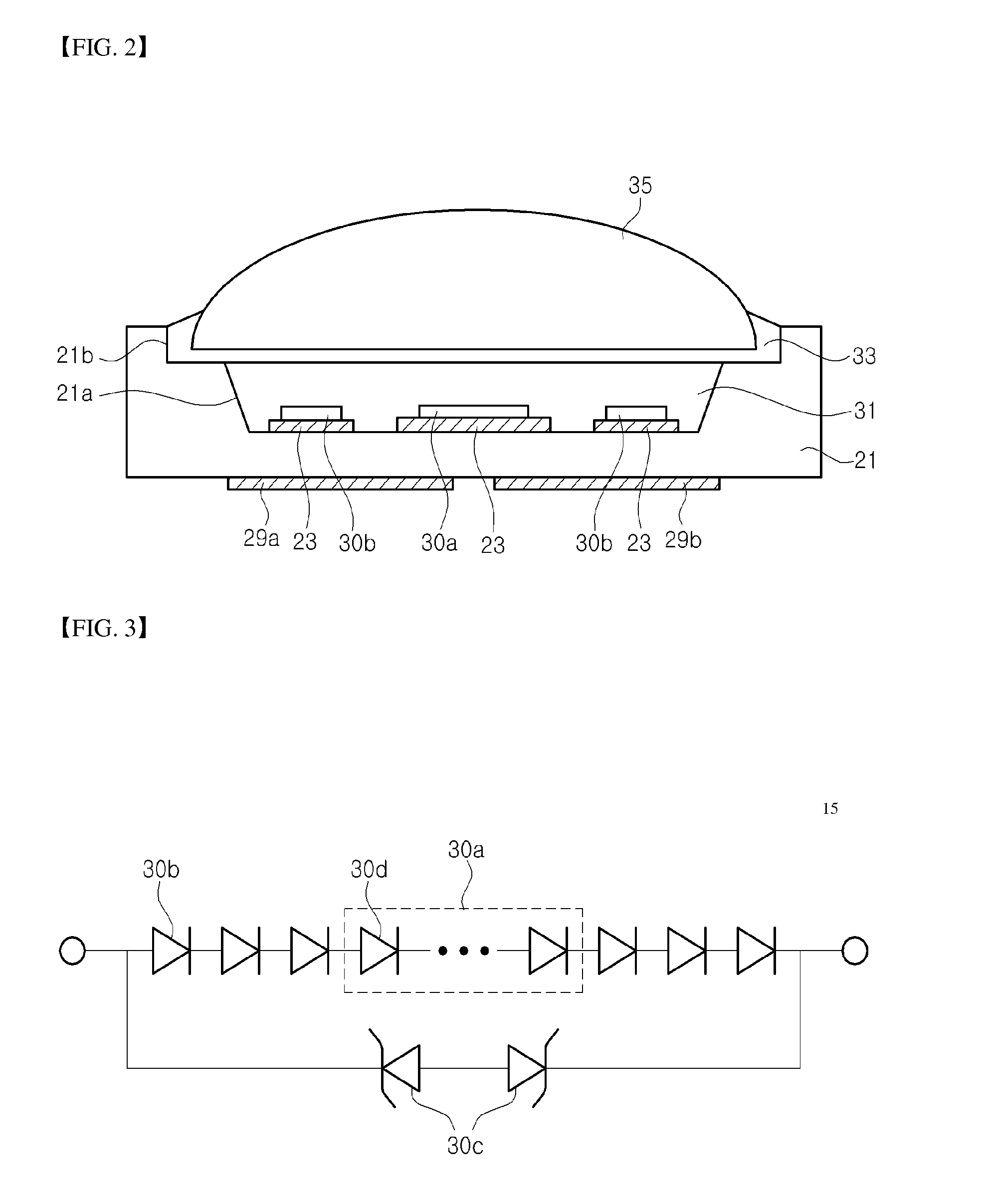
[0052]FIG. 1 is a plan view of a high voltage light emitting diode package in accordance with the present invention, FIG. 2 is a cross-sectional view taken along line A-A of FIG. 1, and FIG. 3 is an equivalent circuit diagram of the light emitting diode package of FIG. 1.

[0053]Referring to FIGS. 1 and 2, the light emitting diode package includes a package body 21, a plurality of landing pads 23, a blue light emitting diode chip 30a, a plurality of red light emitting diode chips 30b, a phosphor, and a pair of lead electrodes 29a, 29b. The light emitting diode package may further include bonding pads 25, 25a, 25b, wires, a molding portion 31, a bonding agent 33, and a lens 35.

[0054]The package body 21 may be formed of ceramics or plastics. Preferably, the package body 21 may be formed of ceramics to ensure thermal resistance and electrical stability. The package body 21 may include a first cavity 21a and a second cavity 21b with a step formed therebetween.

[0055]The landing pads 23 are...

second embodiment

[0074]FIG. 4 is a plan view of a high voltage light emitting diode package in accordance with a second embodiment, FIG. 5 is a cross-sectional view of the high voltage light emitting diode package shown in FIG. 4, and FIG. 6 is a detailed bottom plan view of the high voltage light emitting diode package shown in FIG. 4.

[0075]Referring to FIG. 4, the light emitting diode package of this embodiment includes a package body 121, a plurality of landing pads 123, a blue light emitting diode chip 30a, a plurality of red light emitting diode chips 30b, a phosphor (not shown), and a pair of lead electrodes 129a, 129b. The light emitting diode package may further include bonding pads 125, 125a, 125b and wires W. Although not shown in the drawings, the light emitting diode package of this embodiment may further include a molding portion 31, a bonding agent 33 and a lens 35, as in the above embodiment.

[0076]In this embodiment, the package body 121 has a ceramic stack structure. The ceramic stac...


PUM


Abstract

Disclosed herein is a light emitting diode package including a package body having a cavity, a light emitting diode chip having a plurality of light emitting cells connected in series to one another, a phosphor converting a frequency of light emitted from the light emitting diode chip, and a pair of lead electrodes. The light emitting cells are connected in series between the pair of lead electrodes.

Description

CROSS-REFERENCE TO RELATED APPLICATIONS[0001]This application is the National Stage Entry of International Application PCT / KR2010 / 004222, filed on Jun. 30, 2010, and claims priorities from and the benefit of Korean Patent Application Nos. 10-2009-0060429, filed on Jul. 3, 2009, and 10-2010-0000724, filed on Jan. 6, 2010, all of which are incorporated herein by reference for all purposes as if fully set forth herein.BACKGROUND OF THE INVENTION[0002]1. Field of the Invention[0003]The present invention relates to a light emitting diode package and, more particularly, to a high voltage light emitting diode package that may be operated under a high voltage.[0004]2. Discussion of the Background[0005]Light emitting devices equipped with light emitting diodes, for instance, light emitting diode packages, are widely used not only for applications such as pilot lamps, electronic scoreboards and displays due to its capability of realizing various colors, but also for regular lighting due to ca...

Claims


Application Information

Patent Timeline
IPC IPC(8): H01L33/50H01L33/62H01L33/58
CPCH01L25/0753H01L25/167H01L33/486H01L33/62H01L33/642H01L33/64H01L2224/48227H01L33/58H01L33/48H01L2224/48091H01L2924/00014
Inventor JUNG, JUNG HWAOH, HEETAKKIM, DO HYUNGKWON, YOU JINKIM, OH SUG
Owner SEOUL SEMICONDUCTOR
Why Eureka
Try Eureka