Conductive substrate

a technology of conductive substrate and substrate, which is applied in the field of conductive substrate, can solve the problems of reducing the adhesion property of the interface between the base material and the metal thin film, and achieve the effect of excellent conductivity and high adhesion property

Active Publication Date: 2012-03-15
DAI NIPPON PRINTING CO LTD
View PDF8 Cites 11 Cited by
  • Summary
  • Abstract
  • Description
  • Claims
  • Application Information

AI Technical Summary

Benefits of technology

[0015]The present invention has been made under the situation described above, and an object of the present invention is to provide a conductive substrate which is prepared by forming a metal fine particle sintered film such as a copper wiring and the like on a base material of polyimide and the like and which has a high adhesive property of the metal fine particle sintered film with the base material and is provided with an excellent conductivity and a method for producing the above conductive substrate.
[0016]Intensive investigations repeated by the present inventors in order to achieve the object described above have resulted in finding that a metal thin film can be formed directly on a base material by using a technique in which fine particles of metal and the like are printed on the base material and in which the particles are sintered to form a thin film. On the other hand, involved therein is the problem that even if the above technique is used, an adhesive property of an interface between the base material and the metal thin film is reduced, and it has been found that the cause thereof is attributable to the fact that the particles grow due to aggregation of the particles at the same time as sintering to bring about voids in an interface between the particles and the base material. Further investigations on the fact that the voids are brought about have resulted in finding that a structure in which voids are not brought about in the film and an interface of the base material is formed by sintering the particles for short time before the particles grow due to aggregation of the particles to increase a crystallite diameter obtained from a result of X ray diffraction to 25 nm or more and that an interface between the base material and the metal thin film is smooth and provided with a high adhesive property. Further, it has been found that the higher adhesive property is obtained if organic substances and the like are not present in the metal thin film. The present invention has been completed based on the above knowledge.
[0018]According to the present invention, capable of being provided is a conductive substrate which is prepared by forming a pattern-shaped metal fine particle sintered film such as a copper wiring and the like on a base material of polyimide and the like and which has a high adhesive property with the base material and is provided with an excellent conductivity.

Problems solved by technology

On the other hand, involved therein is the problem that even if the above technique is used, an adhesive property of an interface between the base material and the metal thin film is reduced, and it has been found that the cause thereof is attributable to the fact that the particles grow due to aggregation of the particles at the same time as sintering to bring about voids in an interface between the particles and the base material.

Method used


Image

  • Conductive substrate
  • Conductive substrate
  • Conductive substrate

Examples


example 1

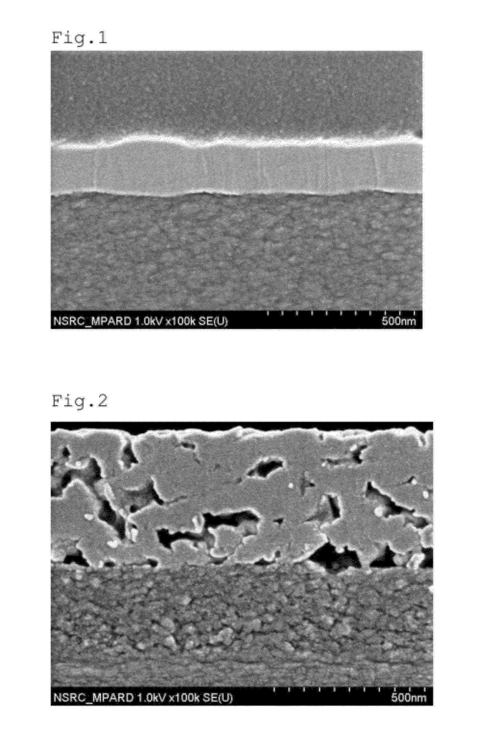
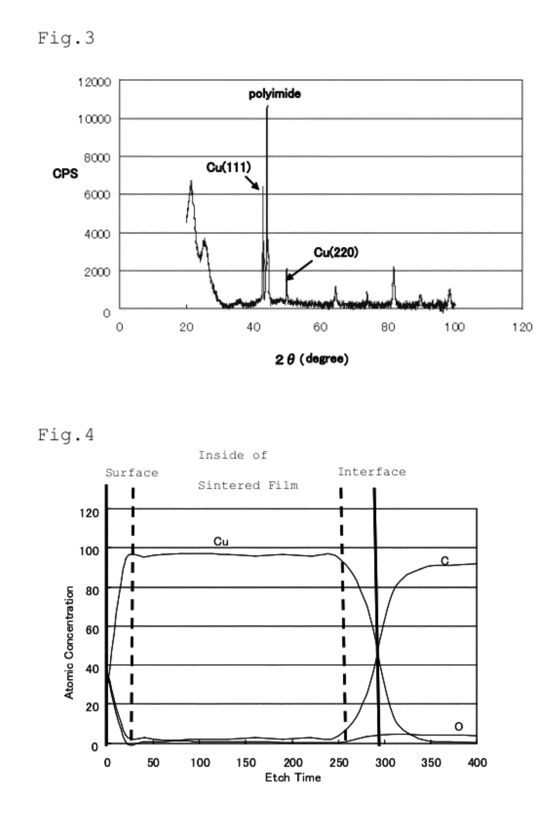
[0073]A toluene dispersion (solid content: 30% by mass, manufactured by ULVAC, Inc.) of copper nanoparticles having an average primary particle diameter of 5 nm was coated on a polyimide film (Kapton 200H, manufactured by Du Pont-Toray Co., Ltd.) having a thickness of 75 μm by a spin coating method, and the coating film was dried naturally. Then, the substrate coated thereon with the copper fine particles was burned in advance at 300° C. for 30 minutes under the air in order to remove organic components.

[0074]Subsequently, the substrate was treated by a microwave surface wave plasma treating equipment (MSP-1500, manufactured by Micro Denshi Co., Ltd.). The plasma treatment was carried out at a hydrogen introducing pressure of 20 Pa, a hydrogen flow amount of 100 sccm and a microwave output of 1000 W using a hydrogen gas for 30 seconds since starting heating. The heating rate was set to about 400° C. / minute, and the reached temperature was set to 230° C.

[0075]The copper nanoparticle ...

example 2

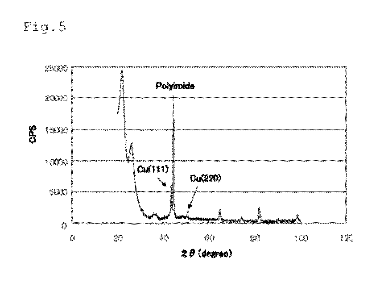
[0079]The same procedure as in Example 1 was carried out, except that the plasma treatment was carried out at a microwave output set to 800 W, a heating rate set to about 320° C. / minute and a reached temperature set to 190° C. The copper nanoparticle sintered film thus obtained was evaluated in the same manner as in Example 1, and the results thereof are shown in Table 1.

example 3

[0080]The same procedure as in Example 1 was carried out, except that the plasma treatment was carried out at a microwave output set to 600 W, a heating rate set to about 250° C. / minute and a reached temperature set to 150° C. The copper nanoparticle sintered film thus obtained was evaluated in the same manner as in Example 1, and the results thereof are shown in Table 1.


PUM

PropertyMeasurementUnit
crystallite diameteraaaaaaaaaa
melting pointaaaaaaaaaa
thicknessaaaaaaaaaa

Abstract

Provided is a conductive substrate which is prepared by forming a pattern-shaped metal fine particle sintered film such as a copper wiring and the like on a base material of polyimide and the like and which has a high adhesive property with the base material and is provided with an excellent conductivity.The conductive substrate of the present invention is prepared by printing a coating liquid containing metal or metal oxide fine particles on a base material to form a print layer and subjecting the above print layer to sintering treatment to form a metal fine particle sintered film, wherein a crystallite diameter in the metal fine particle sintered film which is measured by X ray diffraction is 25 nm or more, and a cross section of the metal fine particle sintered film has a void rate of 1% or less.

Description

BACKGROUND OF THE INVENTION[0001]The present invention relates to a conductive substrate, more specifically to a conductive substrate obtained by printing a coating liquid containing metal or metal oxide fine particles on a base material to form a print layer and subjecting the above print layer to sintering treatment to form a metal fine particle sintered film and a method for producing the above conductive substrate.RELATED ART[0002]A substrate prepared by forming circuit patterns on a base material formed by a polyimide resin has so far been used as a flexible printed wiring board. A method in which a photoresist and the like are coated on a base material comprising a meal foil stuck thereon and exposed to light through a desired circuit pattern to form patterns by chemical etching has so far been used as a method for forming the above circuit patterns.[0003]In the above method, the volume resistivity is small since a metal foil can be used as a conductive wiring, and a conductiv...

Claims


Application Information

Patent Timeline
Patent Type & Authority Applications(United States)
IPC IPC(8): H05K1/09B05D3/02H05K3/00
CPCH05K1/0393H05K2203/1131H05K3/1283
Inventor YOSHI, NAONOBUHOJO, MIKIKO
Owner DAI NIPPON PRINTING CO LTD
Why Eureka
Try Eureka