Sub-threshold memory cell circuit with high density and high robustness

a memory cell, high density technology, applied in the field of memory cells, can solve the problems of weakened writing performance, severe deformation of static noise margin (snm), and deformation of tolerance to process deviation, and achieve optimal write noise margin, high robustness, and overall system performance. high

Active Publication Date: 2012-03-22
SOUTHEAST UNIV
View PDF7 Cites 6 Cited by
  • Summary
  • Abstract
  • Description
  • Claims
  • Application Information

AI Technical Summary

Benefits of technology

[0005]To overcome the drawbacks in the prior art, the present invention provides a high-density and high-robustness sub-threshold memory cell circuit so as to balance the technical indexes of the memory cell and achieve optimal overall system performance. In the present invention, on the basis of the actual characteristics of the sub-threshold circuit, a high-density and high-robustness memory cell with double-end writing and single-end reading features is designed. The memory cell achieves the optimal write noise margin, optimal read noise margin and optimal hold noise margin while requiring extremely low power consumption. In addition, thanks to its high-density design, the chip area consumed by the memory cell array is the smallest among the known chips at present. Thus, that design makes industrialization and commoditization of sub-threshold memory cells possible.
[0008]In above circuit, the NMOS transistors N3 and N4 serve as matching transistors, and the NMOS transistor N5 serves as a cut-off transistor. Since the circuit provided in the present invention is designed for the operation of sub-threshold memory cell, the operating mode of the circuit allows for dynamic switching between the source electrode and the drain electrode in the three transistors N3, N4 and N5, that is to say, the source electrode and drain electrode in the three transistors can be switched over automatically as the variety of potentials at the two connection ends which connected to the said source electrode and drain electrode respectively. Therefore, the source electrode and drain electrode in transistors N3, N4 and N5 can be connected with their corresponding connection ends at random. Compared to the prior art, the present invention has the following advantages and significant effects:
[0009](1) The unit area consumption is the smallest among known sub-threshold memory cells at present. The circuit structure of the seven transistors is simple and reliable. The present invention is less susceptible to process deviations, each transistor is designed in minimum size and has no requirement for proportional design.
[0010](2) The base electrode of P1, P2, and N3˜N5 transistors are connected with the grid electrodes of their corresponding transistor respectively. In the transistors N1 and N2, the base electrode is grounded respectively like the case in the conventional design, therefore, the present invention ensures the balance of the pull-up and pull-down driving capability, while the ON / OFF current of the matching transistor in the memory cell can be increased. Such an arrangement brings two benefits: a) the balanced pull-up and pull-down driving capability ensures robustness of the memory cell. b) the ON / OFF current of the sub-threshold memory cell provided in the present invention is the largest among the sub-threshold memory cells known at present. Thus, the effect of drain current accumulated in unselected memory cells will be reduced. As a result, more memory cells can be supported on the same bit line. Thus, in another aspect, the present invention overcomes a common drawback that only a few of memory cells can be connected in series on the same bit line in existing sub-threshold memory cell arrays so as to increase the capacity and density of sub-threshold memory cell array.
[0011](3) By reading through a single-end read word line (RWL) and writing through a write bit line (WBL) and a NOT WBL ( WBL) at the same time, the present invention achieves a higher read noise margin without lossing the writing performance of the memory cell. Therefore, the memory cell circuit can operate normally without any write-assist unit or sensitive amplifier. Introducing the cut-off transistor N5 is tactfully use the characteristics below that the P-type transistors and N-type transistors in the sub-threshold area transmit complete data signals when |Vgs|>0, but transmit the data signals with loss when |Vgs|=0, which is to say, the cut-off transistor N5 is switched off |Vgs|=0 in the reading cycle so as to prevent disturbance of external information to the internal nodes; the cut-off transistor N5 is switched on |Vgs|>0 in the write cycle and hold cycle so as to enhance writing performance and holding performance.

Problems solved by technology

Memory cell array is an important component in modern digital systems, and is often a bottleneck of power consumption in the system design.
However, in the actual implementation process, the said design introduces a series of problems: 1) the static noise margin (SNM) is degraded severely; 2) the writing performance is weakened; 3) the tolerance to process deviations is degraded, etc.
However, all these designs are implemented at the expense of the density of memory cells.
However, when compared with the conventional six-transistor memory cells, the memory cells in such a structure consume 30% more area.
The approach of making trade-off among reading performance, writing performance and chip area of a memory cell by adjusting the size of transistors in the memory cell in the conventional design (in the super-threshold state) is completely unable to meet the demand of sub-threshold circuit design.
Therefore, the design of high-density and high-robustness sub-threshold memory cell is the bottleneck in the sub-threshold circuit design walking up to industrialization.

Method used


Image

  • Sub-threshold memory cell circuit with high density and high robustness
  • Sub-threshold memory cell circuit with high density and high robustness
  • Sub-threshold memory cell circuit with high density and high robustness

Examples


Embodiment Construction

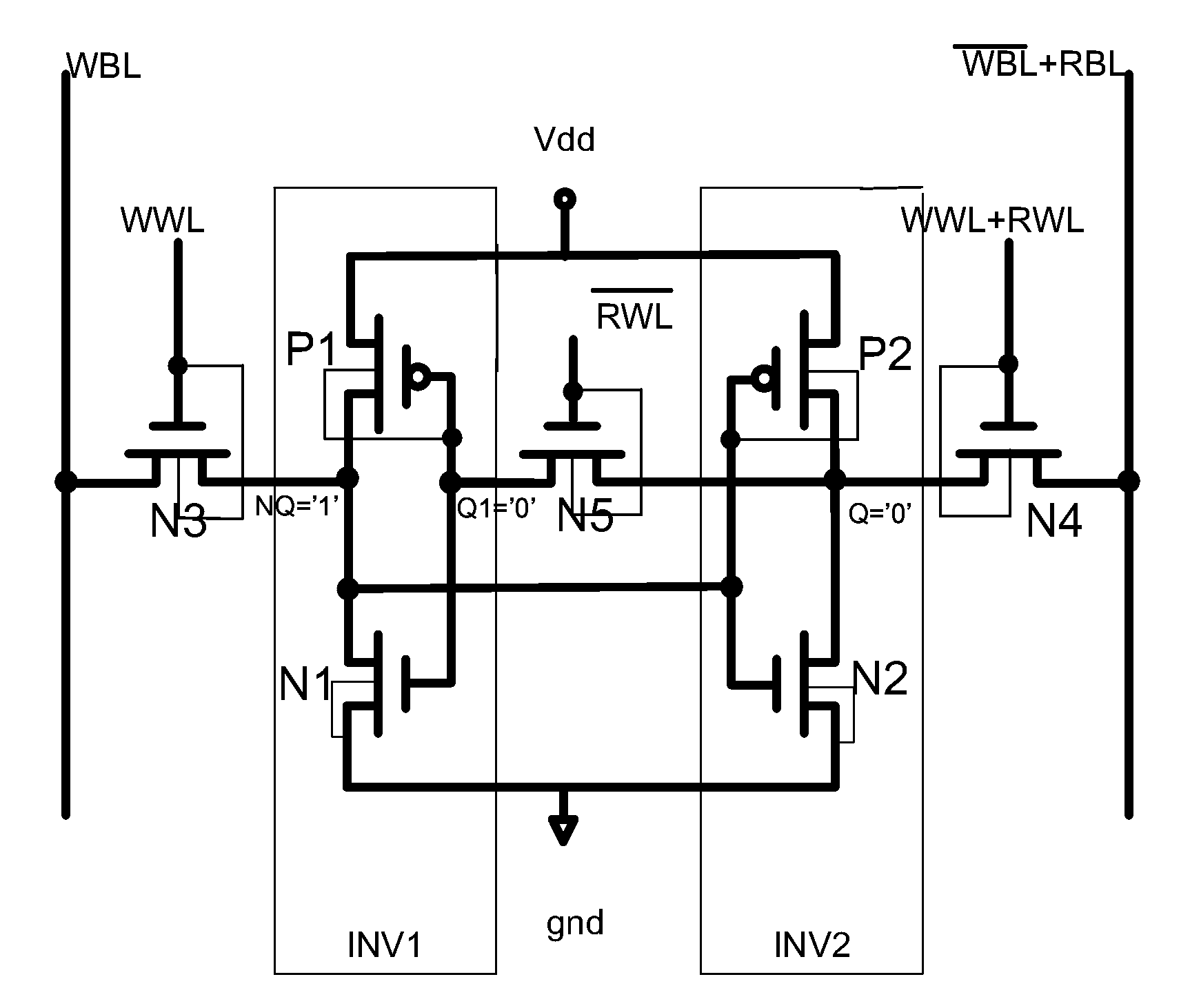
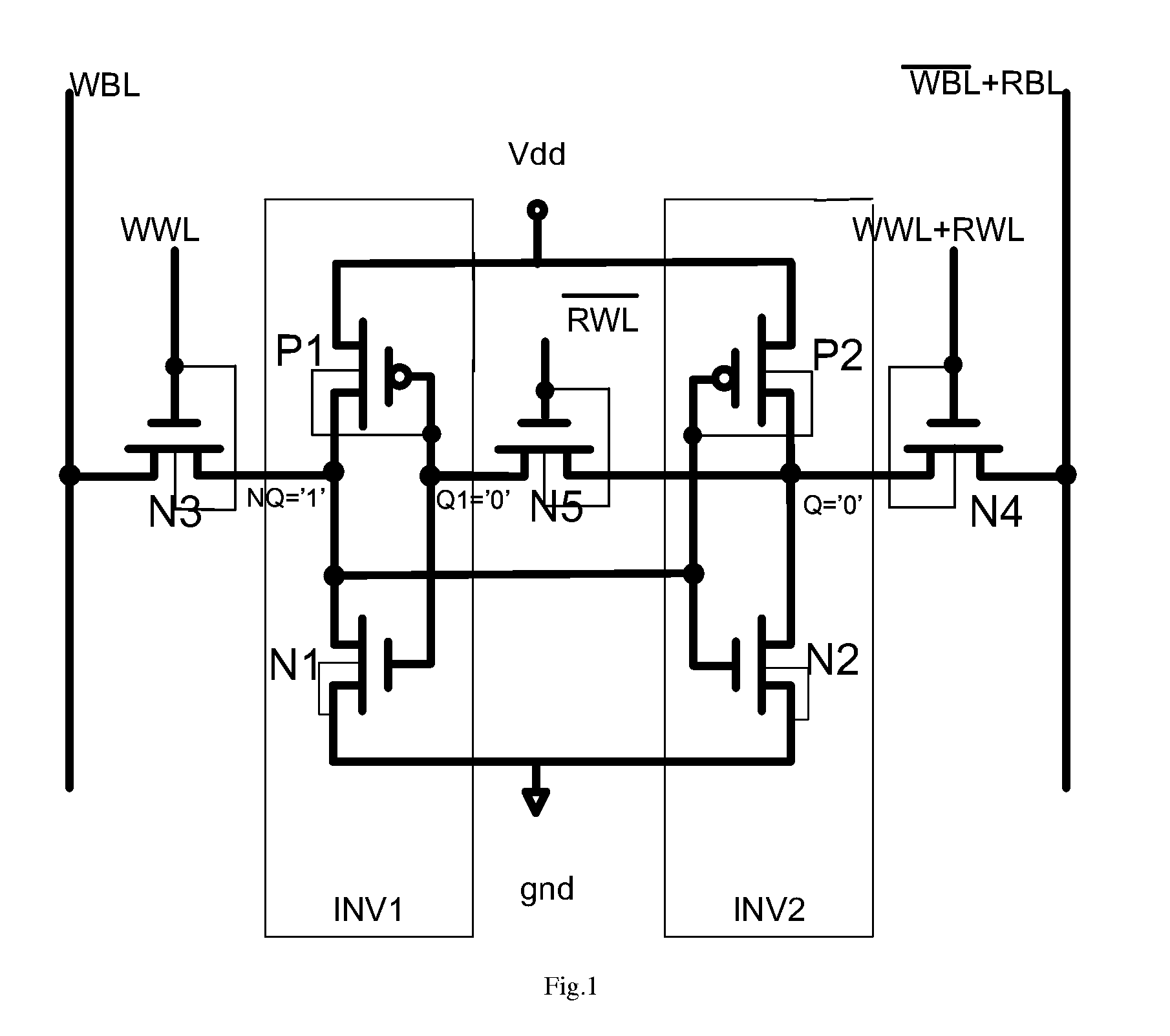
[0017]As shown in FIG. 1, the high-density and high-robustness sub-threshold memory cell circuit provided in the present invention comprises 7 transistors, two P-type transistors (P1,P2) and five N-type transistors (N1˜N5). Wherein, the base electrodes of P1, P2 and N3˜N5 transistor are connected with the grid electrodes of their corresponding transistor respectively. In transistors N1 and N2, the base electrode is connected with the conventional gnd. N1, P1 and N2, P2 form two phase inverters (INV1, INV2) respectively, and the two phase inverters are connected with each other via a cut-off transistor N5 in a cross coupling manner: the output end of INV1 composed of N1 and P1 is directly connected to the input end of INV2 composed of N2 and P2, and the output end of INV2 is connected to the input end of INV1 via the cut-off transistor N5. The grid electrode of N5 is connected with the NEG signal RWL of the read word line (RWL) of external control signal. N3 and N4 are matching trans...


PUM


Abstract

A high-density and high-robustness sub-threshold memory cell circuit, having two PMOS transistors P1 and P2 and five NMOS transistors N1˜N5, wherein, the each base electrode of the two PMOS transistors and NMOS transistors N3, N4, and N5 is connected with the local grid electrode respectively; the base electrode of the NMOS transistors N1 and N2, are grounded respectively; the NMOS transistor N1 form an phase inverter with the PMOS transistor P1, and the NMOS transistor N2 form another phase inverter with the PMOS transistor P2; the two phase inverters are connected with each other in a cross coupling manner via the cut-off NMOS transistor N5, the output end of the phase inverter N1 and P1 directly connected to the input end of the phase inverter N2 and P2, and the output end of the phase inverter N2 and P2 connected to the input end of the phase inverter N1 and P1 via the cut-off NMOS transistor N5; the NMOS transistor N3 is connected with the write bit line (WBL) of the phase inverter N1 and P1, and the NMOS transistor N4 is connected with the NOT WBL and read word line (RWL) of the phase inverter N2 and P2.

Description

FIELD OF THE INVENTION[0001]The present invention relates to a memory cell operating in its sub-threshold working area, particularly to a high-density and high-robustness sub-threshold memory cell circuit. The circuit can operate at 200 mV supply voltage and characterized by the high density, high robustness and extremely low power consumption and so on.BACKGROUND OF THE INVENTION[0002]Memory cell array is an important component in modern digital systems, and is often a bottleneck of power consumption in the system design. As the demand for portable devices increases in the market, it requires higher technique for reducing power consumption in memory cell arrays. Sub-threshold design is a focus in extremely low power design nowadays. By reducing the supply voltage (Vdd) gets into the sub-threshold area of circuit—Vdd is lower than the threshold voltage (Vth), so that the system can operate in the linear range of the circuit, and thereby the dynamic and static power consumption of th...

Claims


Application Information

Patent Timeline
Patent Type & Authority Applications(United States)
IPC IPC(8): G11C11/34
CPCG11C11/412G11C11/34
Inventor YANG, JUNBAI, NALI, JIEHU, CHENSHI, LONGXING
Owner SOUTHEAST UNIV
Why Eureka
Try Eureka