Silicon-germanium heterojunction bipolar transistor

a technology of silicon-germanium heterojunction and transistor, which is applied in the direction of semiconductor devices, basic electric elements, electrical apparatus, etc., can solve the problems of increasing the length of current paths, reducing and reducing the efficiency of the device, so as to shorten the current paths of the device and increase the breakdown voltage of the device. , the effect of reducing resistan

Active Publication Date: 2012-03-29
SHANGHAI HUAHONG GRACE SEMICON MFG CORP
View PDF8 Cites 11 Cited by
  • Summary
  • Abstract
  • Description
  • Claims
  • Application Information

AI Technical Summary

Benefits of technology

[0005]The present invention is to provide a SiGe HBT which is not only capable to increase breakdown voltage of the device, but also can shorten current paths of the device, and reduce the resistance and saturation voltage drop of the device.
[0012]The present invention is capable of: 1) adjusting the breakdown voltage of the device by adjusting the lateral distances between the pseudo buried layers and the active area, in such a way that the breakdown voltage of the device increases with the increase of the lateral distance between each pseudo buried layers and a corresponding edge of the active area; 2) guaranteeing a high breakdown voltage of the device even in the case that a CMOS process with many thermal processes is involved; 3) shortening current paths of the device and reducing resistance by forming N-type implantation regions at the bottom of the second deep hole contacts and thus reducing the saturation voltage drop of the device.

Problems solved by technology

However, once the SiGe HBT is integrated with a CMOS device, thermal processes of the CMOS process will cause the diffusion of the pseudo buried layers, which will lead to a great drop in the breakdown voltage of the device.
However, the above method 3) has a negative effect that the saturation voltage drop of the device will be significantly large, because although the amount of impurities that diffuse into the collector region decreases after the pseudo buried layers are arranged at farther positions, at the same time, the length of the current paths is increased and moreover, as the doping concentration of the lengthened paths are not very high, a large increase in device resistance is resulted.

Method used


Image

  • Silicon-germanium heterojunction bipolar transistor
  • Silicon-germanium heterojunction bipolar transistor

Examples


Embodiment Construction

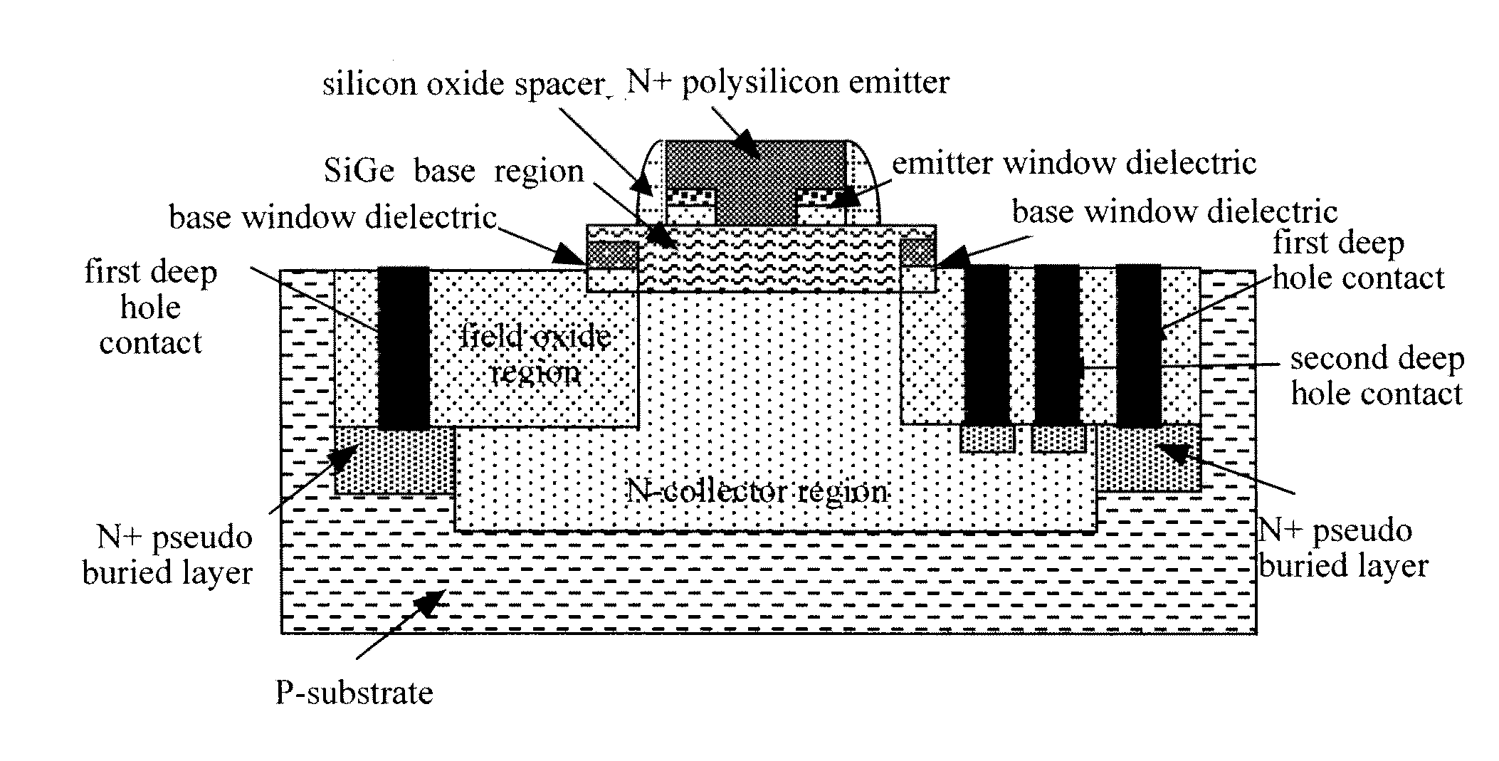
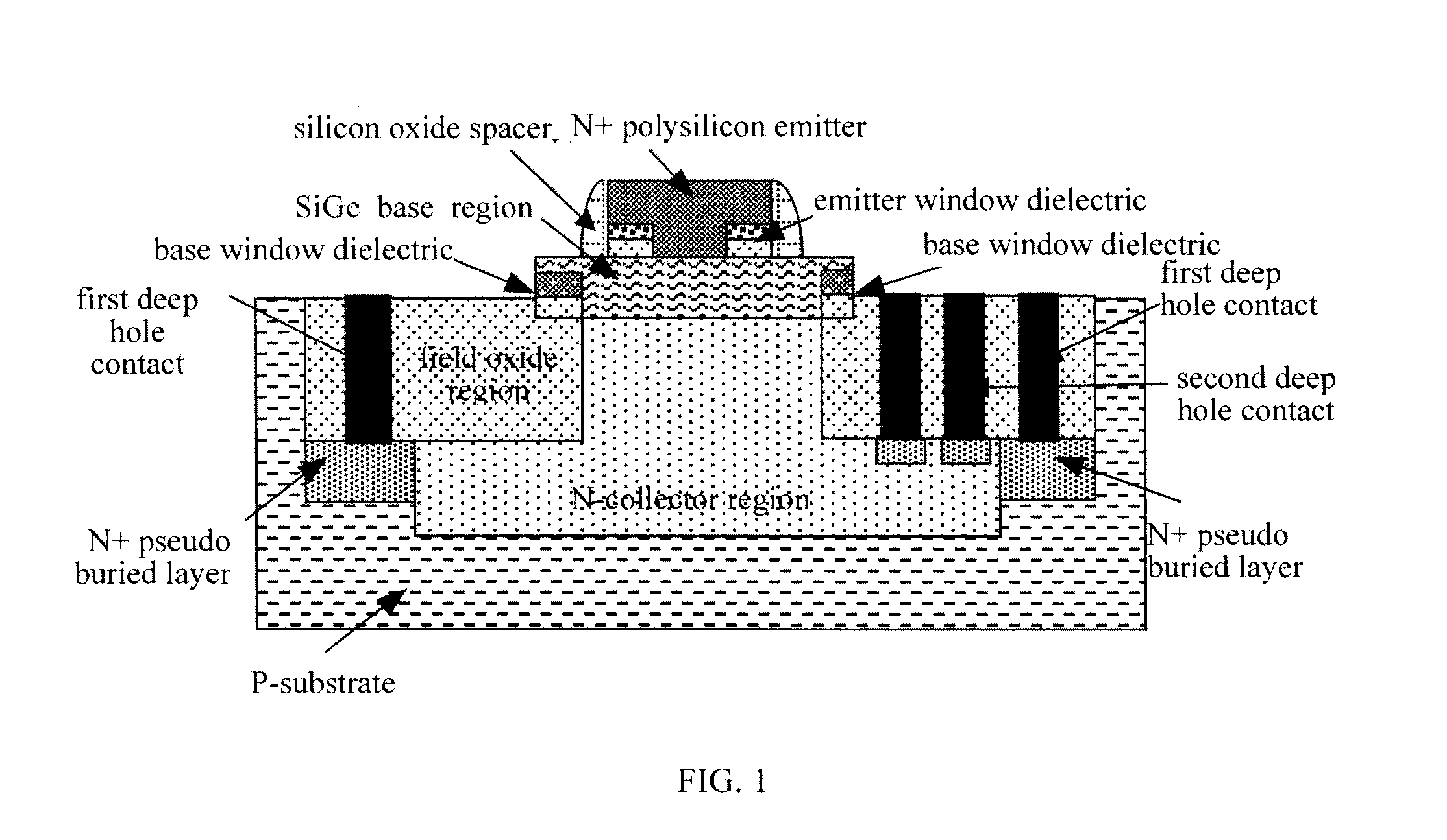
[0015]FIG. 1 shows the structure of the device of an embodiment of the present invention. The SiGe HBT provided by the present invention is formed on a P-type silicon substrate, wherein an active area is isolated by field oxide regions. The SiGe HBT comprises:

[0016]A collector region, shown as the N-collector region in FIG. 1, composed of an N-type ion implantation region formed in the active area, wherein, the collector region has a depth larger than that of the bottom of the field oxide regions and the collector region laterally extends into the bottom of the field oxide regions on both sides of the active area; the N-type ion implantation performed to form the collector region has following process conditions: the implantation dose is from 1e12 to 5e14 cm−2 and the implantation energy is from 50 to 500 KeV.

[0017]Pseudo buried layers, shown as the N+ pseudo buried layers in FIG. 1, composed of N-type ion implantation regions formed at the bottom of the field oxide regions on both ...


PUM


Abstract

A SiGe HBT formed on a silicon substrate is disclosed. An active area is isolated by field oxide regions; a collector region is formed in the active area and extends into the bottom of the field oxide regions; pseudo buried layers are formed at the bottom of the field oxide regions, wherein each pseudo buried layer is separated by a lateral distance from the active area and connected to a lateral extension part of the collector region; first deep hole contacts are formed on top of the pseudo buried layers in the field oxide regions to pick up collector electrodes; a plurality of second deep hole contacts with a floating structure, are formed in the field oxide region on top of a lateral extension part of the collector region, wherein N-type implantation regions are formed at the bottom of the second deep hole contacts.

Description

CROSS-REFERENCES TO RELATED APPLICATIONS[0001]This application claims the priority of Chinese patent application number 201010291766.1, filed on Sep. 26, 2010, the entire contents of which are incorporated herein by reference.TECHNICAL FIELD[0002]The present invention relates to a semiconductor integrated circuit device, and especially relates to a silicon-germanium heterojunction bipolar transistor (SiGe HBT).BACKGROUND OF THE INVENTION[0003]With the increasing maturity of silicon-germanium (SiGe) process, radio-frequency (RF) circuit integration is becoming increasingly commonplace. Such modules as RF receiver, RF transmitter, switch and so on have a tendency towards integration. Therefore, both a low noise amplifier (LNA) for amplifying received signals and a power amplifier (PA) for amplifying the signals to be transmitted should be fabricated on an identical chip, which requires that, on the same SiGe process platform, high-voltage SiGe HBTs with different high breakdown voltag...

Claims


Application Information

Patent Timeline
Patent Type & Authority Applications(United States)
IPC IPC(8): H01L29/737
CPCH01L21/26513H01L29/7378H01L29/41708H01L29/0821
Inventor CHEN, FANCHEN, XIONGBINQIAN, WENSHENGZHOU, ZHENGLIANG
Owner SHANGHAI HUAHONG GRACE SEMICON MFG CORP
Why Eureka
Try Eureka