Epitaxial substrate for electronic device and method of producing the same

a technology of electronic devices and substrates, applied in the direction of semiconductor devices, electrical apparatus, transistors, etc., can solve the problems of increasing power consumption, difficult to make an insulating sic substrate have a higher resistance, and heat generation problems, so as to improve the lateral breakdown voltage characteristics, improve the lateral breakdown voltage, and reduce the lateral leakage current

Active Publication Date: 2012-04-19
DOWA ELECTRONICS MATERIALS CO LTD
View PDF1 Cites 19 Cited by
  • Summary
  • Abstract
  • Description
  • Claims
  • Application Information

AI Technical Summary

Benefits of technology

[0017]An epitaxial substrate for electronic devices according to the present invention includes a buffer having an initial growth layer made of an Al-containing Group III nitride and a given superlattice laminate, and a given main laminate, on a conductive SiC substrate. The superlattice laminate and/or a portion of the main laminate on the buffer side has a C concentration of 1×10¹⁸/cm3 or more, so that not only both decrease in the lateral leakage current and improvement in the lateral breakdown voltage characteristics are successfully achieved, but also vertical breakdown voltage can be improved. Moreover, use of the conductive SiC substrate can improve heat dissipation and reduce crack generation.
[0018]Furthe

Problems solved by technology

Increase of the leakage current increases power consumption, which would consequently cause problems of heat generation and the like.
However, it is difficult to make an insulating SiC substrate have higher resistance in manufacturing the substrate, which would increase the cost.
When a Group III nitride laye

Method used


Image

  • Epitaxial substrate for electronic device and method of producing the same
  • Epitaxial substrate for electronic device and method of producing the same
  • Epitaxial substrate for electronic device and method of producing the same

Examples


experiment example 1

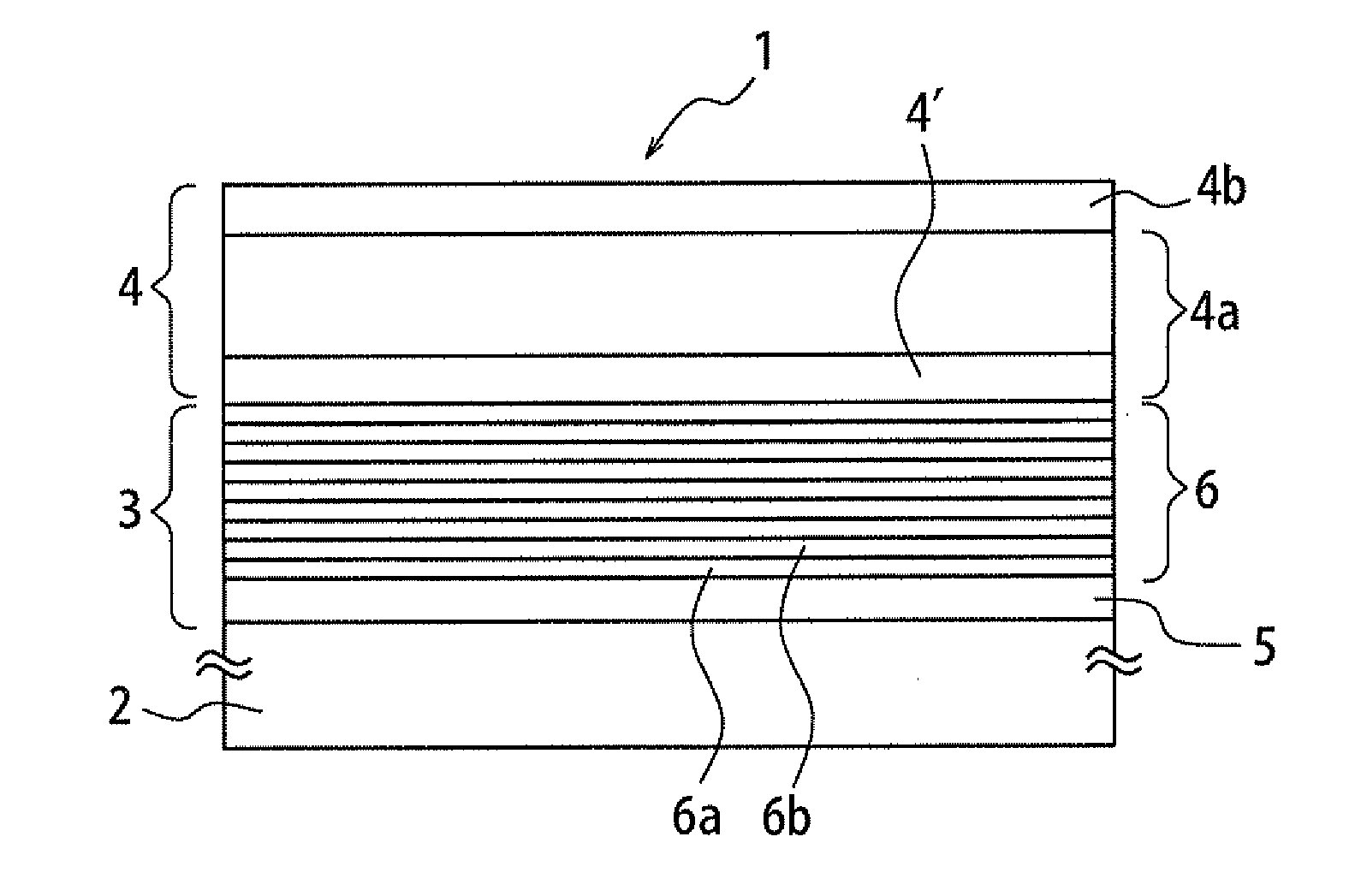
[0042]On each of 300 μm-thick 3 inch 6H—SiC (0001) plane single crystal substrates having a resistivity of 1×10⁻¹ Ω·cm, 10 Ω·cm, and 100 Ω·cm, an initial growth layer (AlN material, thickness: 100 nm) and a superlattice laminate (AlN, film thickness: 4 nm and Al0.15Ga0.85N, film thickness: 25 nm, 85 layers in total) were grown to form a buffer. A channel layer (GaN material, thickness: 1.5 μm) and an electron supply layer (Al0.25Ga0.75N material, thickness: 20 nm) were epitaxially grown on the superlattice laminate to form a main laminate having a HEMT structure. Thus, Samples 1 to 3 were obtained. The concentration of C in the superlattice laminate was changed, and the concentration of C in a portion of the main laminate on the buffer side was in the range of 1.5×10¹⁸ / cm3 to 2.0×10¹⁸ / cm3 in each result. Further, a portion of the channel layer on the electron supply layer side had a C concentration in the range of 0.8×10¹⁶ / cm3 to 3.5×10¹⁶ / cm3. The growth temperature and pressure of ...

experiment example 2

[0051]Samples 4 to 6 were fabricated by similar methods to Samples 1 to 3 in Experiment Example 1 except that the growth pressure of the superlattice laminate was set at 10 kPa, the concentration of C in the portion of the main laminate on the buffer side was changed, and the growth temperature and pressure of each layer were set as shown in Table 2. P2 in the table was controlled to control the C concentration, and the deposition pressure was reduced to increase the C concentration. The concentration of C in the superlattice laminate was in the range of 1.5×10¹⁸ / cm3 to 2.5×10¹⁸ / cm3 in each result.

TABLE 2GrowthGrowthpressuretemperatureLayer(kPa)(° C.)Initial growth layer10700Superlattice laminate101025Channel layer (buffer side)P2 (1-120)1025Channel layer (electron supply layer side)1001075electron supply layer101025

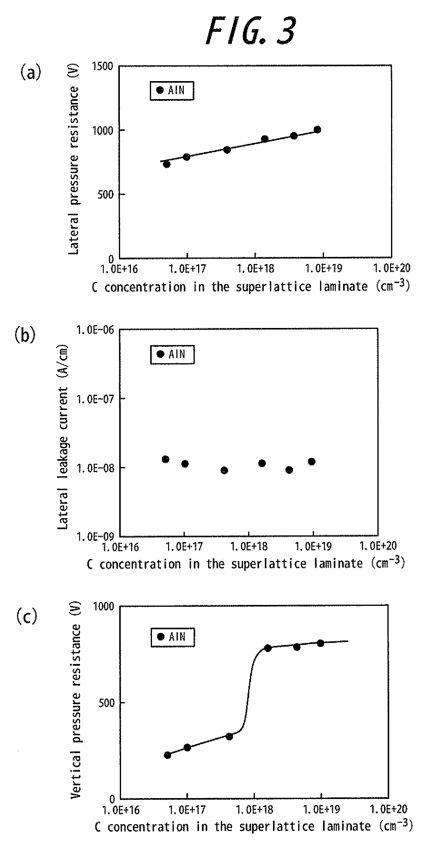
[0052]FIG. 4(a), FIG. 4(b), and FIG. 4(c) show measurement results of the lateral breakdown voltage, the lateral leakage current, and the vertical breakdown voltage of S...

experiment example 3

[0055]Sample 7 was fabricated by a similar method to Sample 2 in Experiment Example 1 except that the initial growth layer was made of a GaN material (thickness: 20 nm) grown at 700° C., and the growth temperature and pressure of each layer were set as shown in Table 3.

TABLE 3GrowthGrowthpressuretemperatureLayer(kPa)(° C.)Initial growth layer10700Superlattice laminateP1 (1-120)1025Channel layer (buffer side)101025Channel layer (electron supply layer side)1001075electron supply layer101025

[0056]When the surface of each epitaxial substrate fabricated in the experiment example was observed under an optical microscope (100 power), many cracks were found to generate. The cracks were generated in the entire surface of the wafer, which made it impossible to fabricate an experimental device.


PUM


Abstract

An epitaxial substrate for electronic devices is provided, which can improve vertical breakdown voltage and provides a method of producing the same.
The epitaxial substrate includes a conductive SiC single crystal substrate, a buffer as an insulating layer on the SiC single crystal substrate, and a main laminate formed by epitaxially growing a plurality of Group III nitride layers on the buffer. Further, the buffer includes at least an initial growth layer in contact with the SiC single crystal substrate and a superlattice laminate having a superlattice multi-layer structure on the initial growth layer. The initial growth layer is made of a Ba1Alb1Gac1Ind1N material. Furthermore, the superlattice laminate is configured by alternately stacking a first layer made of a Ba2Alb2Gac2Ind2N material and a second layer made of a Ba3Alb3Gac3Ind3N material having a different band gap from the first layer.

Description

TECHNICAL FIELD[0001]The present invention relates to an epitaxial substrate for electronic devices and a method of producing the same. The present invention specifically relates to an epitaxial substrate for HEMTs and a method of producing the same.RELATED ART[0002]In recent years, as speed required of IC devices and the like have increased, HEMTs (High electron mobility transistors) have been widely used as high-speed FETs (Field effect transistors). Such a field effect transistor is formed, as schematically illustrated in FIG. 1, for example by stacking a channel layer 22 and an electron supply layer 23 on a substrate 21 and then providing a surface of the electron supply layer 23 with a source electrode 24, a drain electrode 25, and a gate electrode 26. When the device is operated, electrons move through the source electrode 24, the electron supply layer 23, the channel layer 22, the electron supply layer 23, and the drain electrode 25 in this order. A lateral direction is a cur...

Claims


Application Information

Patent Timeline
IPC IPC(8): H01L29/06H01L21/20
CPCH01L21/02378H01L21/02458H01L21/02488H01L21/02507H01L29/7786H01L29/1075H01L29/155H01L29/2003H01L29/207H01L21/0254H01L21/18H01L21/20H01L29/778
Inventor IKUTA, TETSUYASHIMIZU, JOSHIBATA, TOMOHIKOSAKAMOTO, RYOITO, TSUNEO
Owner DOWA ELECTRONICS MATERIALS CO LTD
Why Eureka
Try Eureka