Oxide semiconductor, thin film transistor array substrate and production method thereof, and display device

a thin film transistor and array substrate technology, applied in semiconductor devices, instruments, electrical equipment, etc., can solve the problems of reducing electron mobility, failure to achieve stable tft characteristics, and inability to maintain superior transistor characteristics in some cases, and achieve high-quality images, stable transistor characteristics, and high reliability.

Active Publication Date: 2012-04-19
SHARP KK
View PDF13 Cites 14 Cited by
  • Summary
  • Abstract
  • Description
  • Claims
  • Application Information

AI Technical Summary

Benefits of technology

[0038]The oxide semiconductor of the present invention has a predetermined oxide content. Therefore, if the oxide semiconductor is used for example as a channel layer of a thin film transistor, a highly credible thin film transistor with stable transistor characteristics can be achieved. Moreover, a display device including a thin film transistor array substrate equipped with the thin film transistor can display high quality images. Furthermore, the method of producing a thin film transistor array substrate of the present invention includes a baking treatment performed after formation of a semiconductor layer. As a result, the oxygen content in the semiconductor layer can be easily controlled.

Problems solved by technology

However, if the IGZO semiconductor is applied as a channel layer of a TFT, stable and superior transistor characteristics cannot be maintained in some cases.
As a result, some phenomena occur, such as increase of the off-current, reduction of the electron mobility, and hysteresis in the transistor properties, partly leading to failure to achieve stable TFT characteristics.

Method used


Image

  • Oxide semiconductor, thin film transistor array substrate and production method thereof, and display device
  • Oxide semiconductor, thin film transistor array substrate and production method thereof, and display device
  • Oxide semiconductor, thin film transistor array substrate and production method thereof, and display device

Examples


embodiment 1

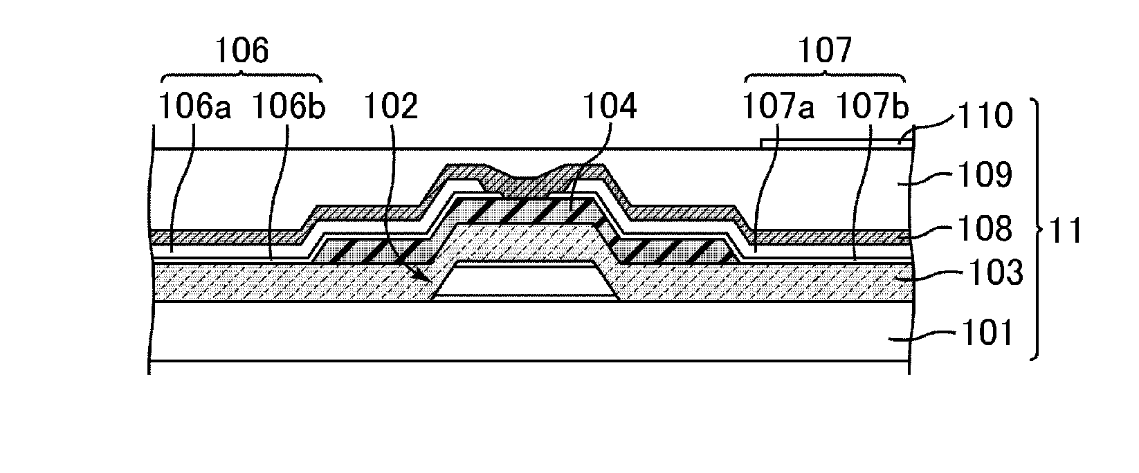
[0054]FIG. 1 is a schematic vertical cross-sectional diagram showing a structure of a pixel of a liquid crystal display device according to the present embodiment. In FIG. 1, a liquid crystal display device 10 is provided with a TFT array substrate 11 having a TFT formed therein, a color filter (CF) substrate 13 as a counter substrate disposed facing the TFT array substrate 11, and a liquid crystal layer 12 sandwiched between the above two substrates.

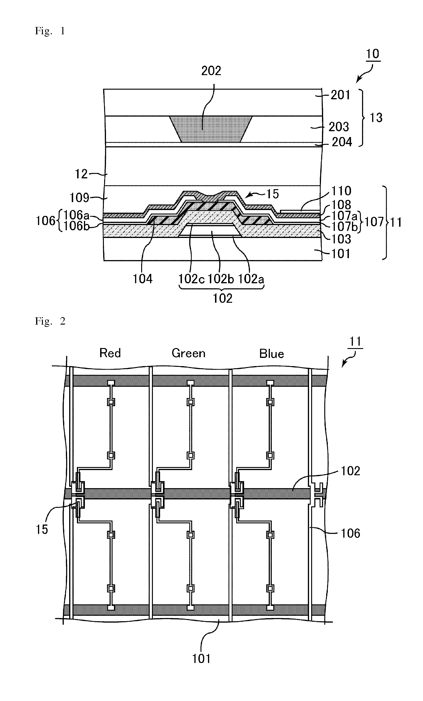
[0055]FIG. 2 is a schematic plain diagram showing the structure of the TFT array substrate 11 in the liquid crystal display device of the present embodiment. In FIG. 2, scanning wirings 102 and signal wirings 106 are disposed in a grid pattern on the main surface of a glass substrate 101. In a plurality of pixel areas which are sectioned by the scanning wirings 102 and the signal wirings 106, TFTs 15 as a switch element are formed in the vicinities of the intersections of the scanning wirings 102 and the signal wirings 106.
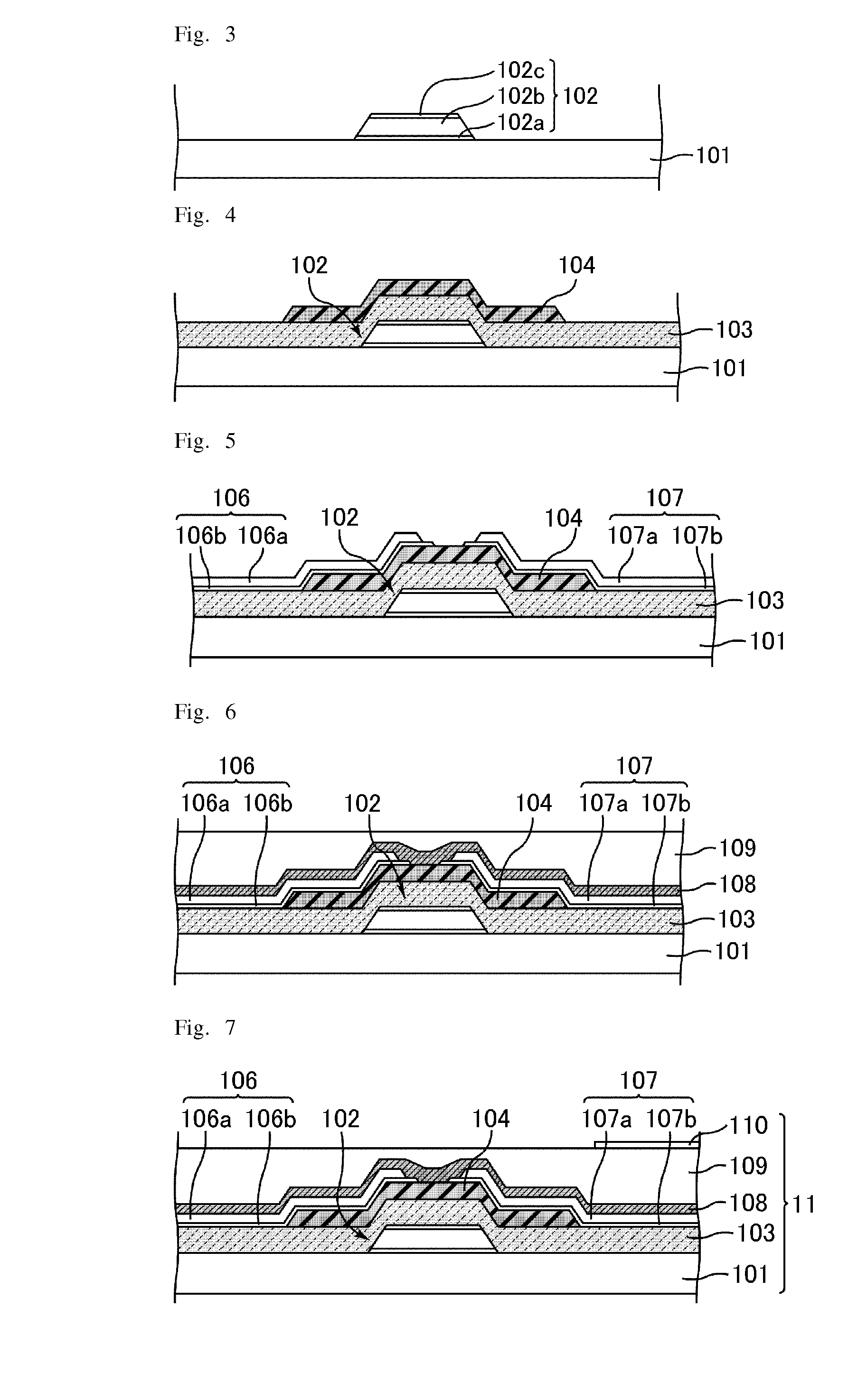
[0056]In a de...

example 1

[0083]In the liquid crystal display device 10 according to the first embodiment, an IGZO semiconductor layer having a thickness of 50 nm was formed by using a sputtering target having the In:Ga:Zn:O ratio=1:1:1:4.

[0084]In order to control the oxygen content of the IGZO semiconductor layer 104, a baking treatment was performed at 350° C. in the atmosphere for one hour after forming the protective layer 108. A clean oven was used herein for the one-hour baking treatment at 350° C. in the atmosphere.

[0085]The composition of the constituent atoms of the IGZO semiconductor layer 104 at a depth of about 20 nm from the surface thereof was measured by AES (Auger Electron Spectroscopy) analysis. The AES analysis was conducted with an AES analyzer (produced by JEOL Ltd., Model No. JAMP-9500F) in the following measurement conditions. Electron irradiation condition: 5 kV, 5 nA; Sample: 75 degrees inclination; Neutralization condition: Ar ion 10 eV, 1 μA; Energy resolution of detector: dE / E=0.35...

example 2

[0097]The composition of the IGZO semiconductor was set to the values shown in the graph in FIG. 11. The baking treatment was performed with a clean oven at 220° C. for one hour in the same manner as in Example 1. Except for the above, various physical characteristic values were measured in the same manner as in Example 1.

[0098]Table 1 and FIG. 13 show the obtained measurement results. FIG. 13 is a graph showing the electric properties of the TFT of the display device in Example 2.


PUM


Abstract

The present invention provides an oxide semiconductor capable of achieving a thin film transistor having stable transistor characteristics, a thin film transistor having a channel layer formed of the oxide semiconductor and a production method thereof, and a display device equipped with the thin film transistor. The oxide semiconductor of the present invention is an oxide semiconductor for a thin film transistor. The oxide semiconductor includes indium, gallium, zinc, and oxygen as constituent atoms, and the oxygen content of the oxide semiconductor is 87% to 95% of the stoichiometric condition set as 100%, in terms of atomic units.

Description

TECHNICAL FIELD[0001]The present invention relates to an oxide semiconductor, a thin film transistor array substrate and a production method thereof, and a display device. Specifically, the present invention relates to an oxide semiconductor suitable as a channel layer of a thin film transistor, a thin film transistor array substrate provided with a thin film transistor having a channel layer formed by including the oxide semiconductor, a production method of the thin film transistor array substrate, and a display device equipped with the thin film transistor array substrate.BACKGROUND ART[0002]Oxide semiconductors are semiconductor materials having higher electron mobility than silicon-based materials such as amorphous silicon (a-Si). For example, it is considered that use of oxide semiconductors for channel layers of thin film transistors (TFT) can produce highly credible TFTs with low leakage current when no voltage is applied. TFTs including oxide semiconductors have thus been d...

Claims


Application Information

Patent Timeline
Patent Type & Authority Applications(United States)
IPC IPC(8): H01L29/786H01L21/34
CPCG02F1/1368H01L29/45H01L29/4908H01L29/66742H01L29/7869H01L29/22H01L21/02565H01L21/02631G02F2202/10H01L29/66969H01L21/02554
Inventor OHTA, YOSHIFUMIMORI, GONISHIKI, HIROHIKOCHIKAMA, YOSHIMASAAITA, TETSUYASUZUKI, MASAHIKONAKAGAWA, OKIFUMITAKEI, MICHIKOHARUMOTO, YOSHIYUKIHARA, TAKESHI
Owner SHARP KK
Why Eureka
Try Eureka