Photonic crystal pressure sensor

a pressure sensor and photonic crystal technology, applied in the field of pressure sensors, can solve the problems of difficult to achieve, practical limitations likely preclude its application in real-world devices, and spectral detuning of the microcavity resonance, so as to increase the evanescent coupling and reduce the optical transmission

Inactive Publication Date: 2012-04-26
UNIV OF WESTERN ONTARIO
View PDF6 Cites 20 Cited by
  • Summary
  • Abstract
  • Description
  • Claims
  • Application Information

AI Technical Summary

Benefits of technology

[0008]The present invention provides a microscale pressure sensor comprising a bridged device in which a photonic crystal waveguide, surrounded by a photonic crystal slab, is suspended over a dielectric substrate. Under applied pressure, the photonic crystal waveguide is deflected toward the substrate, causing a decrease in optical transmission across the waveguide due to the coupling of the evanescent field of the guided mode to the dielectric substrate. In a preferred embodiment, the waveguide is coupled to a photonic crystal microcavity, which increases evanescent coupling.

Problems solved by technology

The principle of operation of the device involved the effect of strain on the refractive index of the structure, which was shown to cause the spectral detuning of the microcavity resonance.
While this structure succeeds in theoretically demonstrating sensitivity to pressure, practical limitations likely preclude its application in real-world devices.
Firstly, the sensitivity of the device depends on a very high quality factor for the microcavity, which is known to be extremely difficult to achieve in microstructured photonic crystal devices due to limitations in material processing technology.
Secondly, the device requires a high spectral resolution for the measurement of pressure, which may limit the range of applications for the device.

Method used


Image

  • Photonic crystal pressure sensor
  • Photonic crystal pressure sensor
  • Photonic crystal pressure sensor

Examples


example 1

Fabrication of Device in Silicon-on-Insulator Wafer

[0067]Devices according to a preferred embodiment of the invention are preferably fabricated as follows. The top pattern of device, including the photonic crystal region and conventional waveguides, is created onto silicon-on-insulator (SOI) wafers via electron beam lithography. The SOI wafers, typically 4″ or 6″ in diameter, may be purchased from a commercial supplier and diced to 1.5 cm×1.5 cm square wafer pieces. A 200 nm thick uniform layer of e-beam resist (ZEP520A) is coated on the wafer. Standard electron beam lithography is used to write the photonic crystal pattern in the resist. The resist pattern is developed and then transferred onto the device layer, Silicon, by inductively coupled plasma etching, also known as dry etching. To obtain smooth sidewalls in the holes, cryogenic dry etch process is used. The Bosch process can also be used to etch the holes but will have more roughness which can affect the waveguide loss. The...

example 2

Optical Modelling of Line Defect

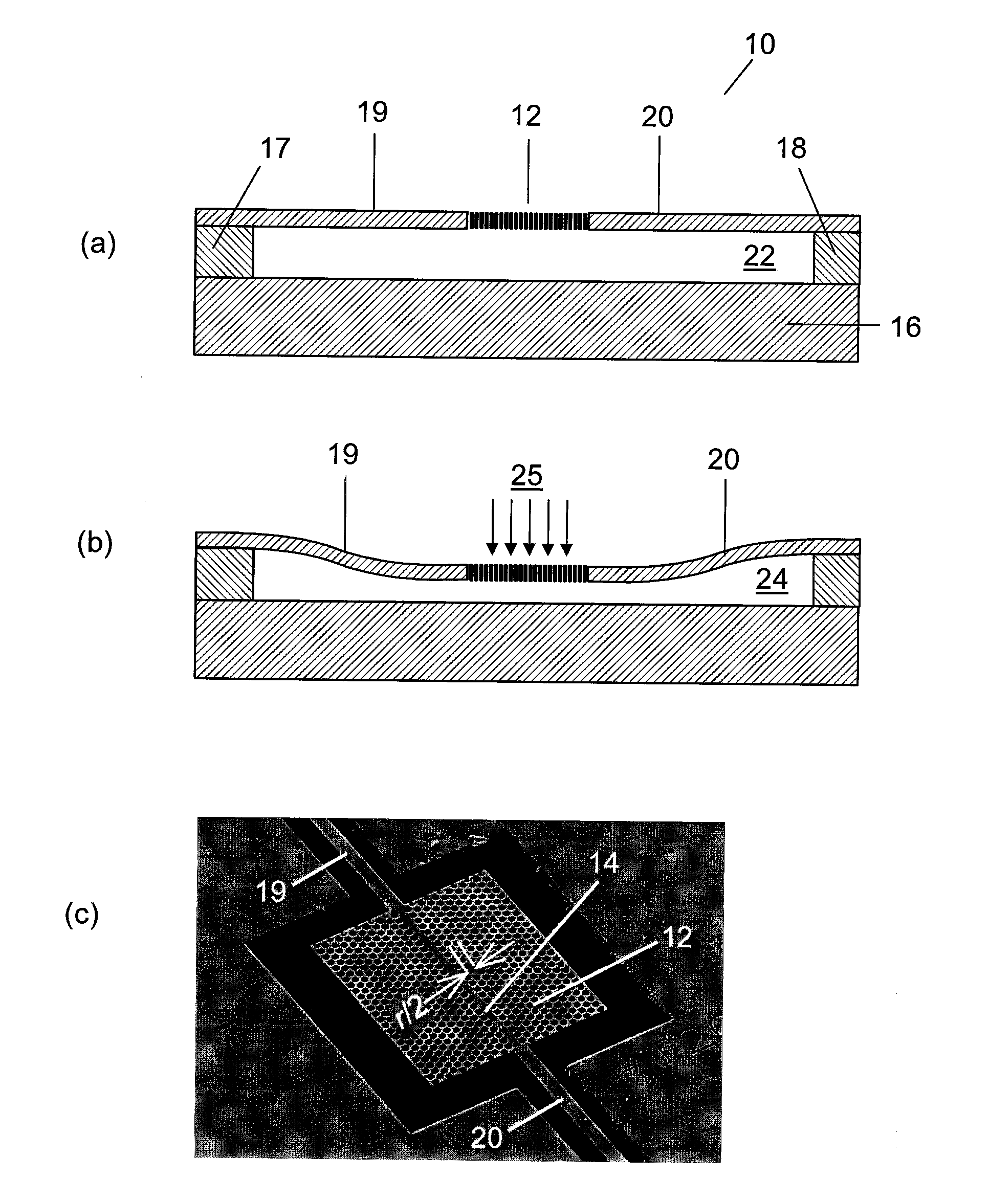
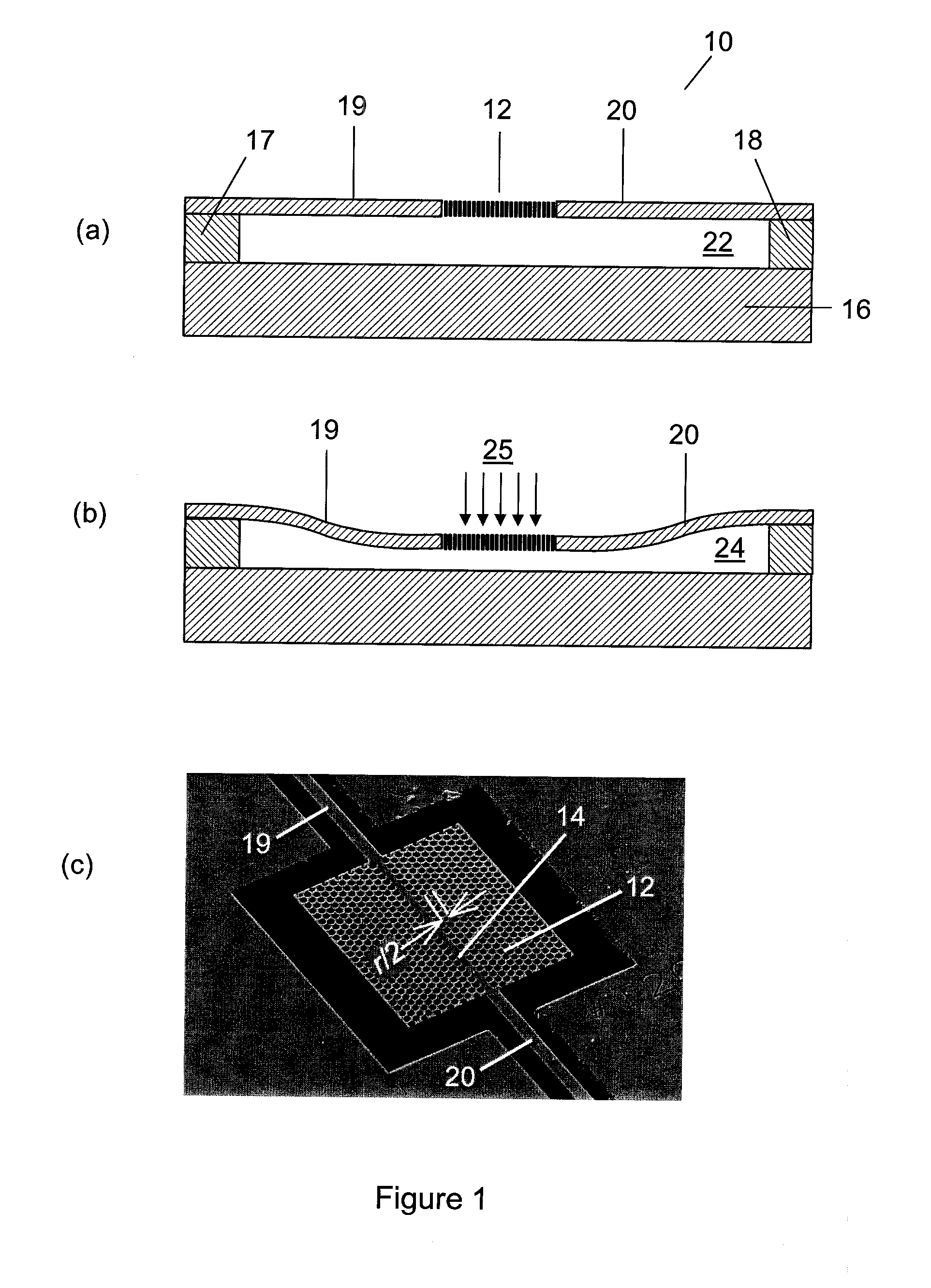
[0070]A line defect photonic crystal waveguide was modelled with broad transmission bandwidth from 1.23 μm to 1.53 μm and high transmission coefficient of over 80%. Transmission was measured between the conventional output to input waveguides of the suspended bridge. The polarization was TM (Electric field parallel to the photonic crystal slab). The lattice type was hexagonal with a lattice constant of 400 nm and a hole diameter of 280 nm. The geometrical parameters of the bridge were as follows: slab thickness=300 nm, bridge width=1300 nm, bridge length=20 μm (along the propagation direction) and the best conventional waveguide width that minimizes coupling loss to the photonic crystal section was found to be 800 nm.

[0071]By inserting a microcavity next to the photonic crystal waveguide (highlighted as r / 2 in FIG. 1(c)), strong coupling occurs between the photonic crystal waveguide and the cavity near resonance frequency that taps some of the propaga...

example 3

Mechanical Modelling of Line Defect

[0074]In addition to the optical modelling of the photonic crystal structure, it is useful to relate the optical performance to the mechanical response of the photonic crystal pressure sensor. The measurement of mechanical properties of photonic crystal devices is often challenging due to the miniaturized structure and need for accurate force control.

[0075]In order to perform a physical characterization relating the effect of forces applied at different points on the sensor to the spectral response of the sensor, a sufficiently small and precise tool is required. Considering the small size of the photonic crystal materials, the source of the force could be of sharp shape, such as the tip of an atomic force microscope or atomic force microscope cantilever.

[0076]Atomic force microscopes can be operated in air, different gases, vacuum, or liquid [8]. Force volume mode is used to acquire the curves of applied force vs. vertical distance for each point ...


PUM

PropertyMeasurementUnit
gap distanceaaaaaaaaaa
dielectric constantaaaaaaaaaa

Abstract

The present invention provides a microscale pressure sensor that exhibits high sensitivity in a small form factor. The sensor is a bridged device in which a photonic crystal waveguide, surrounded by a photonic crystal slab, is suspended over a dielectric substrate. Under applied pressure, the photonic crystal waveguide is deflected toward the substrate, causing a decrease in optical transmission across the waveguide due to the coupling of the evanescent field of the guided mode to the dielectric substrate. In a preferred embodiment, the waveguide is coupled to a photonic crystal microcavity, which increases evanescent coupling.

Description

CROSS-REFERENCE TO RELATED APPLICATION[0001]This application claims priority to U.S. Provisional Application No. 61 / 213,050, titled “PHOTONIC CRYSTAL PRESSURE SENSOR” and filed on May 1, 2009, the entire contents of which are incorporated herein by reference.FIELD OF THE INVENTION[0002]The present invention relates to pressure sensors. More particularly, the present invention relates to microscale optical pressure sensors incorporating photonic crystals.BACKGROUND OF THE INVENTION[0003]Within the past decade, photonic crystals, also referred to as photonic band gap materials [1], have emerged as a new class of materials and devices providing remarkable capabilities of light control and manipulation. The possibility to modify dynamically the geometrical parameters of the photonic crystal structure makes possible the realization of sensitive optical device and thus the 2D photonic crystal technology extremely attractive for the fabrication of physical sensors [1,2,3,4].[0004]Sensors n...

Claims


Application Information

Patent Timeline
Patent Type & Authority Applications(United States)
IPC IPC(8): G01L1/00G01L9/00H01L21/02
CPCG01L9/0076
Inventor SABARINATHAN, JAYSHRIBAKHTAZAD, AREFHUO, XUANHUTTER, JEFF
Owner UNIV OF WESTERN ONTARIO
Why Eureka
Try Eureka