Vertical organic field effect transistor and method of its manufacture

a transistor and organic field technology, applied in transistors, solid-state devices, nano-informatics, etc., can solve the problems of low working frequency, low mobility of organic materials, low on-current,

Active Publication Date: 2012-04-26
TECHNION RES & DEV FOUND LTD
View PDF1 Cites 17 Cited by
  • Summary
  • Abstract
  • Description
  • Claims
  • Application Information

AI Technical Summary

Problems solved by technology

However, the organic materials suffer from low mobility compared to inorganic materials.
This difference of five to six orders of magnitude is the cause of the disadvantages of these devices, low ON-current, high active voltage and low working frequency.
This transistor utilizes, for the source electrode, a highly non uniform film in that it has thin and thick regions.
However, this transistor design suffers from the need to produce the source electrode with a finely tuned roughness (i.e., optimization of thin versus thick properties of the film), which lowers reproducibility of these results.
These devices, however, relied on an ultra-thin (<20 nm) aluminum source electrode that required careful partial oxidation.
While such devices exhibited about 6 orders of magnitude current modulation, the low work-function aluminum source electrode required an n-type active channel restricting the device to the use of C60 as the channel material.

Method used


Image

  • Vertical organic field effect transistor and method of its manufacture
  • Vertical organic field effect transistor and method of its manufacture
  • Vertical organic field effect transistor and method of its manufacture

Examples


Embodiment Construction

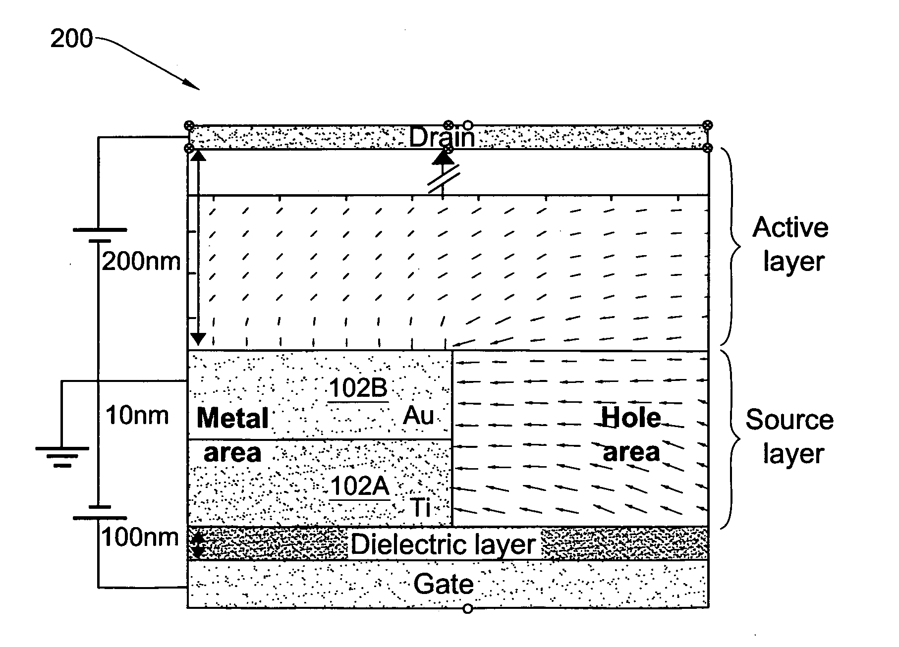
[0063]The present invention provides an electrically-conductive perforated patterned structure enclosed between a dielectric layer and an active element of the electronic device and having a geometrical pattern defining an array of spaced-apart perforation regions surrounded by electrically conductive regions (grid). The active element is in direct contact with the dielectric layer within the perforation regions. A material composition of the device and features of said geometrical pattern are selected to provide a desired electrical conductance of the electrically-conductive perforated patterned structure and a desired profile of a charge carriers' injection barrier along said structure.

[0064]The desired profile of the charge carriers' injection barrier is selected such that the charge injection barrier is lower for the area closer to the active layers gate dielectric layer and higher on the upper interface of the patterned electrode.

[0065]For example, the electrode thickness may b...


PUM


Abstract

An electronic device (100) is presented, being configured for example as a vertical field effect transistor. The device comprises an electrically-conductive perforated patterned structure (102) which is enclosed between a dielectric layer (105) and an active element (106) of the electronic device (100). The electrically-conductive perforated patterned structure (102) comprises a geometrical pattern defining an array of spaced-apart perforation regions (108) surrounded by continuous electrically conductive regions (110). The pattern is such as to allow the active element (106) of the electronic device (100) to be in direct contact with said dielectric layer (105) aligned with the perforation regions (108). A material composition of the device (100) and features of said geometrical pattern are selected to provide a desired electrical conductance of the electrically-conductive perforated patterned structure (102) and a desired profile of a charge carriers' injection barrier along said structure (102).

Description

FIELD OF THE INVENTION[0001]This invention is in the field of organic field effect transistors (OFETs), and relates to a vertical-design OFET and a method of its manufacture.REFERENCES[0002]The following references are considered to be pertinent for the purpose of understanding the background of the present invention:[0003]1. L. P. Ma and Y. Yang, “Unique architecture and concept for high-performance organic transistors,” Applied Physics Letters, vol. 85, pp. 5084-5086,2004.[0004]2. Volker Abetz, Peter F. W. Simon “Phase Behavior and Morphologies of Block Copolymers”, Adv Poly. Sci. 189: 125-212 (2005)[0005]3. V. Castelletto, I. W. Hamley, “Morphologies of block copolymer melts” Solid State and Materials Science 8 (2004) 426-438[0006]4. A. Tapponnier, I. Biaggio, and P. Gunter, “Ultrapure C60 field-effect transistors and the effects of oxygen exposure” APPL. PHYS. LET. 86, 112114 (2005)[0007]5. Liping Ma and Y. Yang, “Solid-state supercapacitors for electronic device applications” A...

Claims


Application Information

Patent Timeline
Patent Type & Authority Applications(United States)
IPC IPC(8): H01L29/786H01L21/302
CPCB82Y10/00H01L21/3086H01L51/0023H01L51/0046H01L51/0055H01L51/057H01L29/78696H01L51/5203H01L27/12H01L27/1214H01L29/66757H01L29/66765H01L51/102H10K71/621H10K85/211H10K85/623H10K10/491H10K10/82H10K50/805
Inventor TESSLER, NIRBEN-SASSON, ARIEL
Owner TECHNION RES & DEV FOUND LTD
Why Eureka
Try Eureka