Connecting material, semiconductor device and method for manufacturing semiconductor device
Active Publication Date: 2012-04-26
HITACHI LTD
View PDF18 Cites 6 Cited by
Summary
Abstract
Description
Claims
Application Information
AI Technical Summary
This helps you quickly interpret patents by identifying the three key elements:
Problems solved by technology
Method used
Benefits of technology
[0024]These and other objects, features and advantages of the invention will be apparent from the following mor
Problems solved by technology
Therefore, sufficient wetting cannot be obtained without breaking the oxide film mechanically.
In this case, even if connecting could be attained, the connection is made just very locally, so that an obtainable connecting strength is very weak and not suitable for practical use of the solder.
If pressurizing is needed when connecting even with a low load applied, the mass production cost increases significantly, and thereby, its application to some products may be difficult.
A conventional con
Method used
Image
Click on the blue label to locate the original text in one second.
Reading with bidirectional positioning of images and text.
Examples
embodiment 1
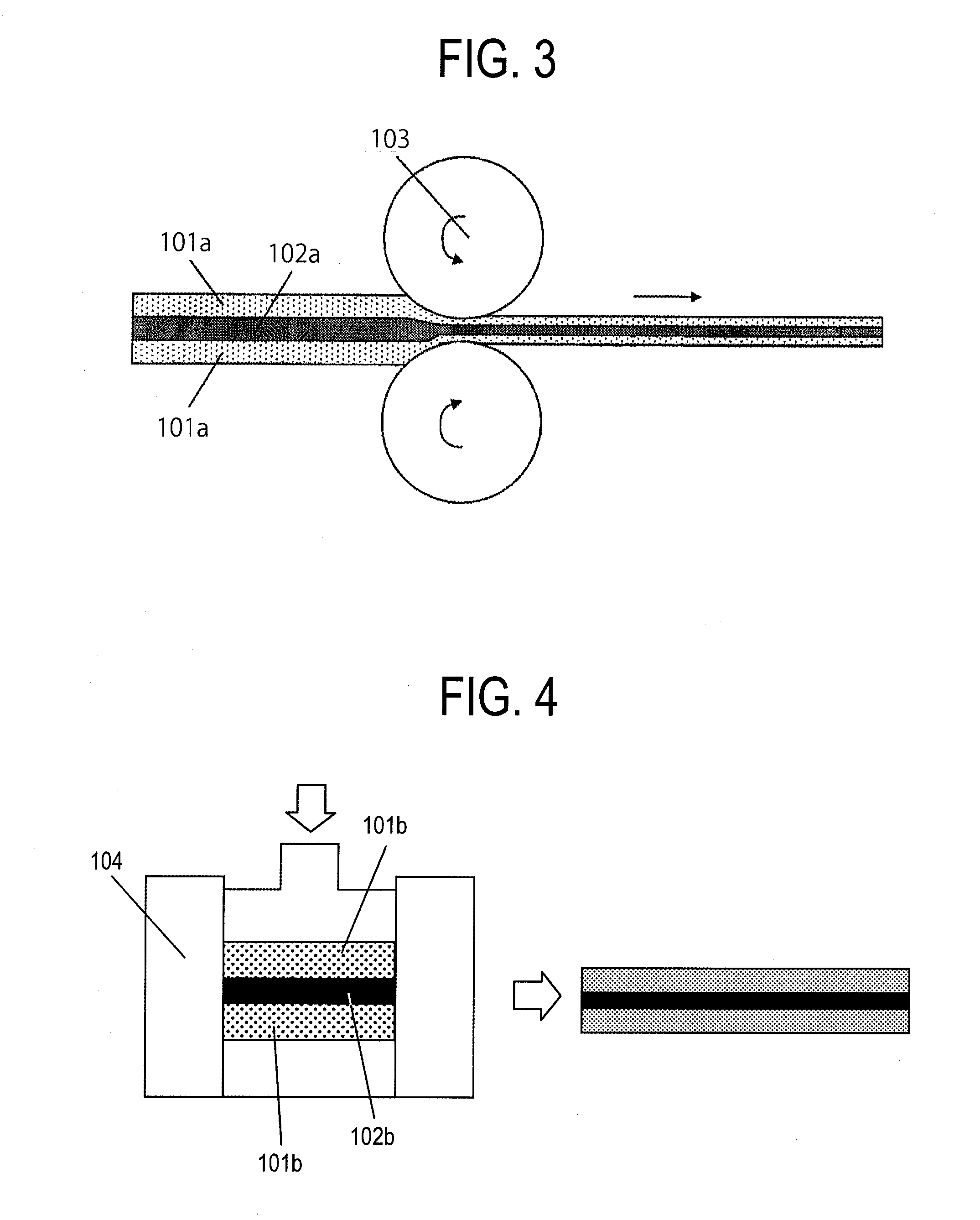
[0066]FIG. 6 is a table showing thickness of respective layers of cladding materials (cladding materials 1 to 8) used in this working example. For example, cladding material 1 has a Zn layer of 19 μm in thickness, an Al layer of 10 μm in thickness, and a Zn layer of 19 μm in thickness. Thicknesses of other cladding materials are denoted in a similar manner. Here, cladding materials 1 to 4 represent connecting materials used in the working example of the present invention, while cladding materials 5 to 7 represent connecting materials used as comparative examples.
[0067]Zn / Al / Zn cladding materials used in the working example described hereinafter were fabricated by using a method for manufacturing a connecting material shown in FIG. 3 or FIG. 4.
working examples 1 to 12
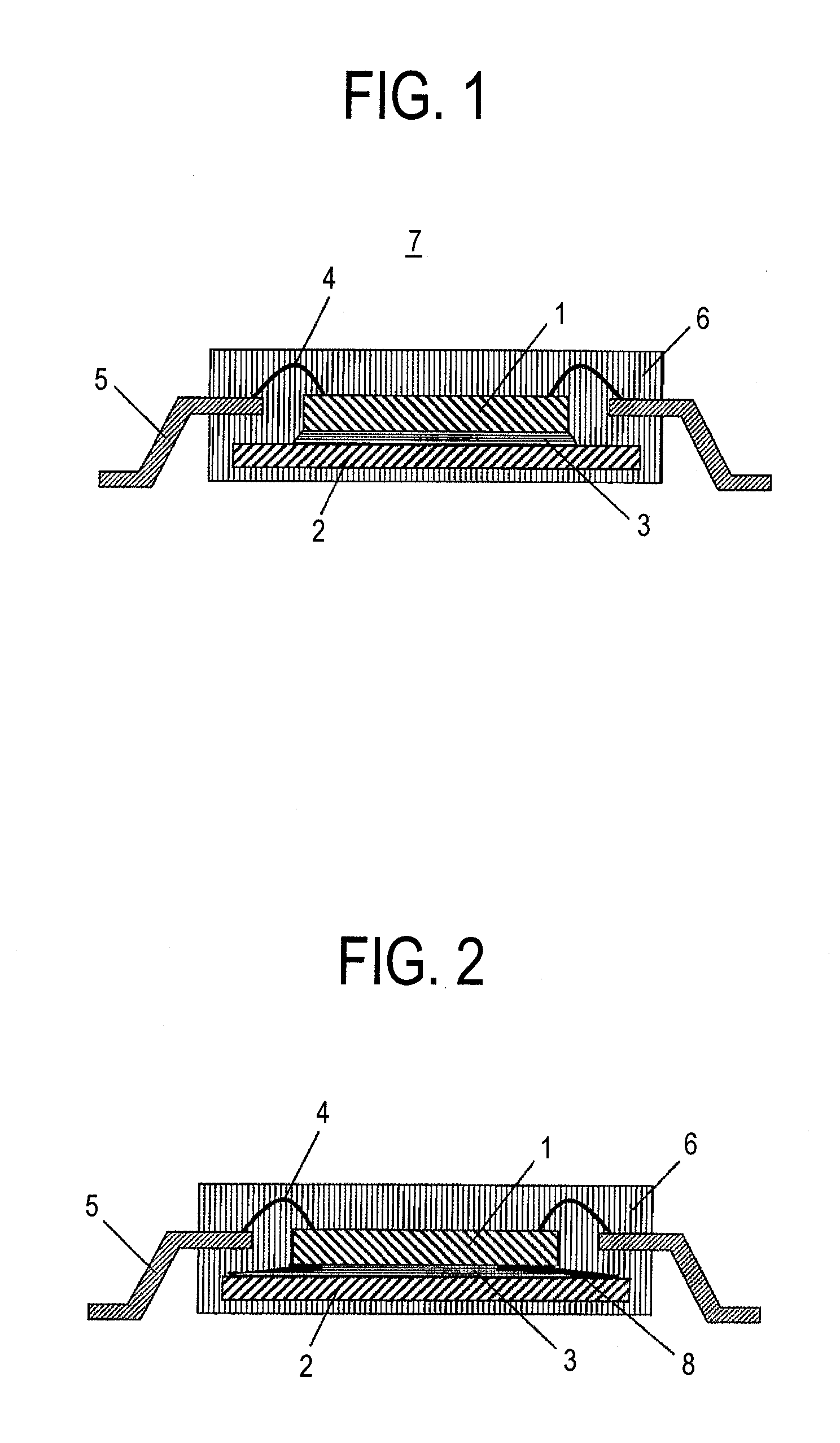
[0068]FIG. 7 is a view showing an example of a semiconductor device according to Embodiment 1 of the present invention. A semiconductor device 11 includes a semiconductor element 1, a frame 2 to which the semiconductor element 1 is connected, a lead 5 with one end thereof serving as an external terminal, a wire 4 which connects another end of the lead 5 to an electrode of the semiconductor element 1, and a sealing resin 6 which resin-seals the semiconductor element 1 and the wire 4, wherein the semiconductor element 1 and the frame 2 are connected to each other via a connecting part 10.
[0069]A connecting material fabricated by a manufacturing method shown in FIG. 3 or FIG. 4 was placed between the semiconductor element 1 and the frame 2, and the semiconductor device 11 was die-bonded via the connecting part 10 by using the connecting material shown in FIG. 3 or FIG. 4.
[0070]Next, a method for manufacturing the semiconductor device 11 shown in FIG. 7 is described. The semiconductor d...
working examples 13 to 24
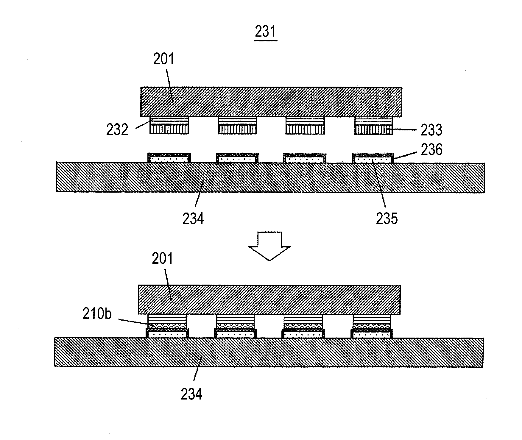
[0077]FIG. 11 is a view showing an example of a semiconductor device according to an embodiment of the present invention. As shown in FIG. 11, working examples 13 to 24 are connected by using a connecting material shown in FIG. 3 or FIG. 4 as a sealing material of the semiconductor device 21 which requires hermetical sealing. The semiconductor device 21 includes a semiconductor element 1, a module substrate 23 to which the semiconductor element 1 is connected, a lead 5 with one end thereof serving as an external terminal, and a wire 4 which connects another end of the lead 5 and an electrode of the semiconductor 1, wherein the semiconductor 1 and the wire 4 were hermetically sealed, the semiconductor element 1 and the chip components were connected to the module substrate 23 by using an Sn-based lead-free solder 3, a conductive adhesive, a Cu powder / Sn-based solder powder composite, or the like, and a connecting material 10a was placed between the module substrate 23 and the metal c...
PUM
Property
Measurement
Unit
Temperature
aaaaa
aaaaa
Fraction
aaaaa
aaaaa
Fraction
aaaaa
aaaaa
Abstract
When connecting with a conventional Zn/Al/Zn cladding material, thickness of a connecting part needs to be less than double an existing high-lead solder (about 100 μm) in order to make heat resistance in the connecting part at least equivalent to a level of the existing solder. Moreover, thickness of an Al layer needs to make as thick as possible in order to fully exhibit stress relaxation performance of the Al layer.
Provided is a semiconductor device including a semiconductor element, a frame, and a connecting part which connects the semiconductor element and the frame to each other, in which an interface between the connecting part and the semiconductor element and an interface between the connecting part and the frame respectively have the area of Al oxide film which is more than 0% and less than 5% of entire area of the respective interfaces.
Description
BACKGROUND[0001]The present invention relates to a connecting material and a semiconductor device.[0002]Adverse effects of the lead against human nerves and hematogenic systems have been proved. In Europe, the ELV Directive (End-of Life Vehicles Directive) restricting the use of a lead in vehicles and the RoHs (Restriction of the use of certain Hazardous Substances in electrical and electronic equipment) prohibiting the use of a lead in electrical and electronic equipment have been put in force in October, 2000 and in July, 2006 respectively. Conventionally, solders used for electric connections of components of electrical and electronic equipment contained the lead. Depending on the melting point, solders are classified into three types including a high temperature solder, a medium temperature solder, and a low temperature solder. Medium temperature solders such as Sn—Ag—Cu based solder, Sn—Cu based solder, and the like, and low temperature solders such as Sn—Bi based solder, Sn—In...
Claims
Application Information
Patent Timeline
Application Date:The date an application was filed.
Publication Date:The date a patent or application was officially published.
First Publication Date:The earliest publication date of a patent with the same application number.
Issue Date:Publication date of the patent grant document.
PCT Entry Date:The Entry date of PCT National Phase.
Estimated Expiry Date:The statutory expiry date of a patent right according to the Patent Law, and it is the longest term of protection that the patent right can achieve without the termination of the patent right due to other reasons(Term extension factor has been taken into account ).
Invalid Date:Actual expiry date is based on effective date or publication date of legal transaction data of invalid patent.