Semiconductor memory device and driving method thereof

a memory device and semiconductor technology, applied in the field of memory devices, can solve the problems of failure to respond, extremely unstable output potential in this region, loss of data, etc., and achieve the effects of reducing power consumption, reducing power consumption, and reducing power consumption

Active Publication Date: 2012-04-26
SEMICON ENERGY LAB CO LTD
View PDF2 Cites 31 Cited by
  • Summary
  • Abstract
  • Description
  • Claims
  • Application Information

AI Technical Summary

Benefits of technology

[0032]An object of one embodiment of the present invention is to provide a semiconductor memory device with less power consumption at the time of data retention. Another object of one embodiment of the present invention is to provide a semiconductor memory device in which

Problems solved by technology

Here, if the on-resistances of the selection transistors STr1 and STr2 are too low, the output potentials of the inverters are affected by the potential of the bit line, so that the flip-flop circuit becomes unstable, which may results in loss of data.
However, since both of them have high resistance, output potential VOUT in this region is extremely unstable and fails to respond in short time.
Therefore, when a load is connected to the output of the inverter, output potential of the inverter may drastically change regardless of the input of the inverter.
In addition, as a result of the miniaturization of the transistors, statistic

Method used


Image

  • Semiconductor memory device and driving method thereof
  • Semiconductor memory device and driving method thereof
  • Semiconductor memory device and driving method thereof

Examples


embodiment 1

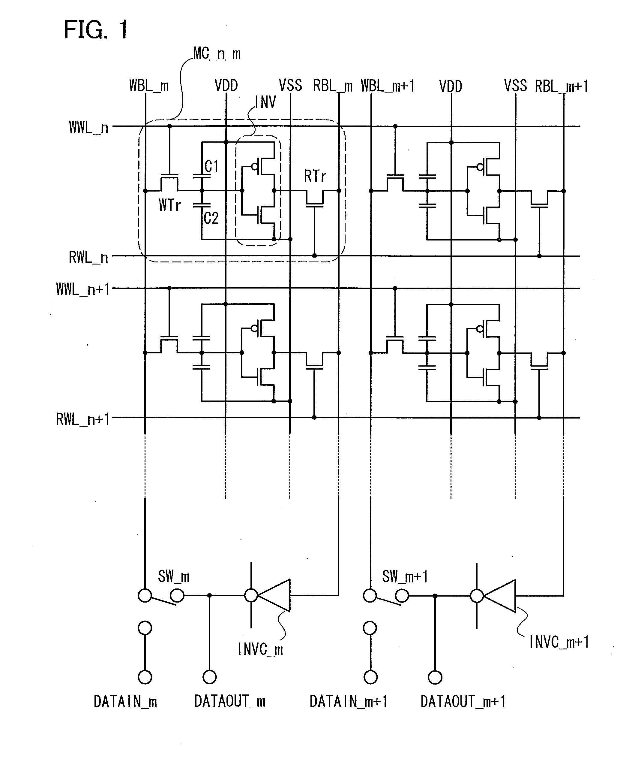
[0072]In this embodiment, the semiconductor memory device in FIG. 1 and an operational example thereof will be described with reference to FIGS. 3A to 3F. A semiconductor device in this embodiment includes write word lines WWL, read word lines RWL, write bit lines WBL orthogonal to the write word lines, read bit lines RBL orthogonal to the read word lines, and memory cells.

[0073]FIG. 1 illustrates a memory cell in the n-th row and m-th column, a memory cell in the (n+1)-th row and m-th column, a memory cell in the n-th row and the (m+1)-th column, and a memory cell in the (n+1)-th row and (m+1)-th column, and the write word lines WWL, read word lines RWL, write bit lines WBL, and read bit lines RBL which relate to these memory cells.

[0074]Each memory cell includes a write transistor WTr, a read transistor RTr, an inverter INV, and capacitors C1 and C2. The capacitor C1 or the capacitor C2, or both may be provided unintentionally.

[0075]The drain of the write transistor WTr is connect...

embodiment 2

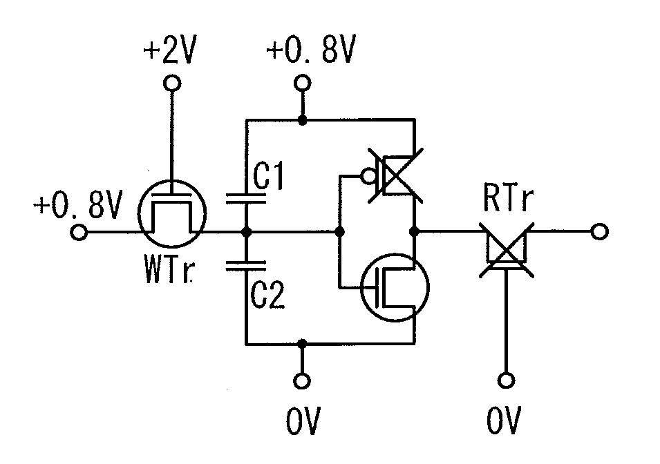
[0117]This embodiment will be described with reference to FIG. 1 and FIGS. 4A to 4C. In the writing method in Embodiment 1, during the write operation, the write transistor WTr is turned on by operating the write word line WWL, so that all the write transistors WTr connected to one write word line WWL are turned on. Consequently, charges stored on the capacitors connected to the sources of all the write transistors WTr in that row is lost.

[0118]This embodiment will give the description of a method in which data are rewritten to only, of the memory cells connected to the write word line WWL, ones in the columns that need to be rewritten, and the same data as those stored before are automatically written to the others.

[0119]FIGS. 4A to 4C show an example. Here, the potential of the positive electrode of the inverter INV is +0.8 V, and the potential of the negative electrode of the inverter INV is 0 V. As illustrated in FIG. 4A, for the memory cell in the n-th row and the m-th column (...

embodiment 3

[0130]In this embodiment, modified examples of the semiconductor memory device in FIG. 1 will be described with reference to FIGS. 5A to 5C. In the memory cell illustrated in FIG. 5A, the write bit line for the adjacent memory cell is used as a substitute of the read bit line. In other words, the bit line BL_m+1 is the read bit line for the memory cell in the n-th row and the m-th column (MC_n_m) and also the write bit line for the memory cell in the n-th row and the (m+1)-th column.

[0131]In the memory cell in FIG. 5B, the write bit line used for this memory cell is a substitute of the read bit line. In other words, the bit line BL_m the read bit line for the memory cell in the n-th row and the m-th column and also the write bit line used for this memory cell.

[0132]The memory cell in FIG. 5C is one in which the inverter is not a complementary inverter but a resistive load inverter. In other words, a resistor R is used instead of the p-type transistor in the inverter INV_n_m included...


PUM


Abstract

In a memory cell, a transistor with extremely high off-resistance is used as a write transistor; a drain and a source of the write transistor are connected to a write bit line and an input of an inverter, respectively; and a drain and a source of a read transistor are connected to a read bit line and an output of the inverter, respectively. Capacitors may be intentionally disposed to the source of the write transistor. Alternatively, parasitic capacitance may be used. Since the data retention is performed using charge stored on these capacitors, a potential difference between power sources for the inverter can be 0. This eliminates leakage current between the positive and negative electrodes of the inverter, thereby reducing power consumption.

Description

BACKGROUND OF THE INVENTION[0001]1. Field of the Invention[0002]The present invention relates to a memory device using a semiconductor.[0003]2. Description of the Related Art[0004]A static random access memory (an SRAM) using two inverters for its memory cell operates at high speed, and thus is used to temporarily store programs and / or data either in the CPU or in a part near the CPU. Unlike a dynamic random access memory (a DRAM), the SRAM does not require to be refreshed while storing data, thereby consuming less power in standby mode. For this reason, the SRAM is also used for data storage in a portable device.[0005]FIG. 2A illustrates a conventional SRAM memory cell. The memory cell is connected to two bit lines BL1 and BL2 and one word line WL. The memory cell includes two selection transistors STr1 and STr2 and two inverters INV1 and INV2. The gates of the selection transistors STr1 and STr2 are connected to the word line WL. The drain of the selection transistor STr1 is conne...

Claims


Application Information

Patent Timeline
IPC IPC(8): G11C5/10G11C5/06
CPCG11C11/412
Inventor TAKEMURA, YASUHIKO
Owner SEMICON ENERGY LAB CO LTD
Why Eureka
Try Eureka