Photonics module and method of manufacturing

a technology of photonic modules and manufacturing methods, applied in the direction of manufacturing tools, semiconductor lasers, instruments, etc., can solve the problems of requiring operator skill, high cost equipment, and relative long time to manufacture, and achieve the effects of low cost, minimal optical coupling loss, and high optical power

Inactive Publication Date: 2012-04-26
PALOMAR MEDICAL TECH
View PDF3 Cites 28 Cited by
  • Summary
  • Abstract
  • Description
  • Claims
  • Application Information

AI Technical Summary

Benefits of technology

[0031]It is desirable to design a photonics module that is suitable for application in a device having a lower price point relative to current devices that incorporate photonics module(s). It is desirable that this lower cost photonics module achieves relatively high optical power (greater then 1 W, greater than 0.5 W, or from about 0.5 W to about 20 W, or greater than 20 W) with minimal optical coupling loss (e.g., an optical coupling loss that is less than about 15%, or less than about 12%, or less than about 10%, or less than about 5%). It is desirable for a lower cost photonics module(s) to have one or more of, fewer parts less bill of material (BOM), a lower cost of bill of material (cBOM) and / or a lower manufacturing cost (e.g., a lower cost manufacturing process and / or a lower cost apparatus for assembly of a photonics module).

Problems solved by technology

Currently, photonics modules having relatively high optical power (e.g., greater than 1 W) and relatively lower optical coupling loss (e.g., less than about 15% optical coupling loss) take a relatively long time to manufacture, require operator skill, and require operator intervention and / or high cost equipment to manufacture, and are, accordingly, relatively costly to manufacture.
It is particularly desirable to use a diode laser and a submount material that have similar thermal expansion characteristics when a hard solder is employed to mount the diode laser to the submount, otherwise there is a risk of stress caused by a mismatch of these thermal expansion characteristics that could degrade the lifetime and / or performance of the diode laser.
Hence, the maximum takt time in the entire assembly sequence limits the capacity the line is capable of producing.
The alignment and attachment step is time consuming.
The process of gluing the FAC lens to the submount is time consuming and requires skill since the optical power and beam pattern must be monitored throughout the cure process, with corrections being made by a skilled operator to compensate for movement of the FAC lens while the glue (e.g., the epoxy) cures.
Alternatively, the process of gluing the lens to the submount requires sophisticated automated equipment to achieve the desired optical power and beam pattern and the process still remains time consuming.
The choice or selection of solder is limited by the glass transition temperature of the fiber cladding and / or by the glass transition temperature of the buffer.

Method used


Image

  • Photonics module and method of manufacturing
  • Photonics module and method of manufacturing
  • Photonics module and method of manufacturing

Examples


Embodiment Construction

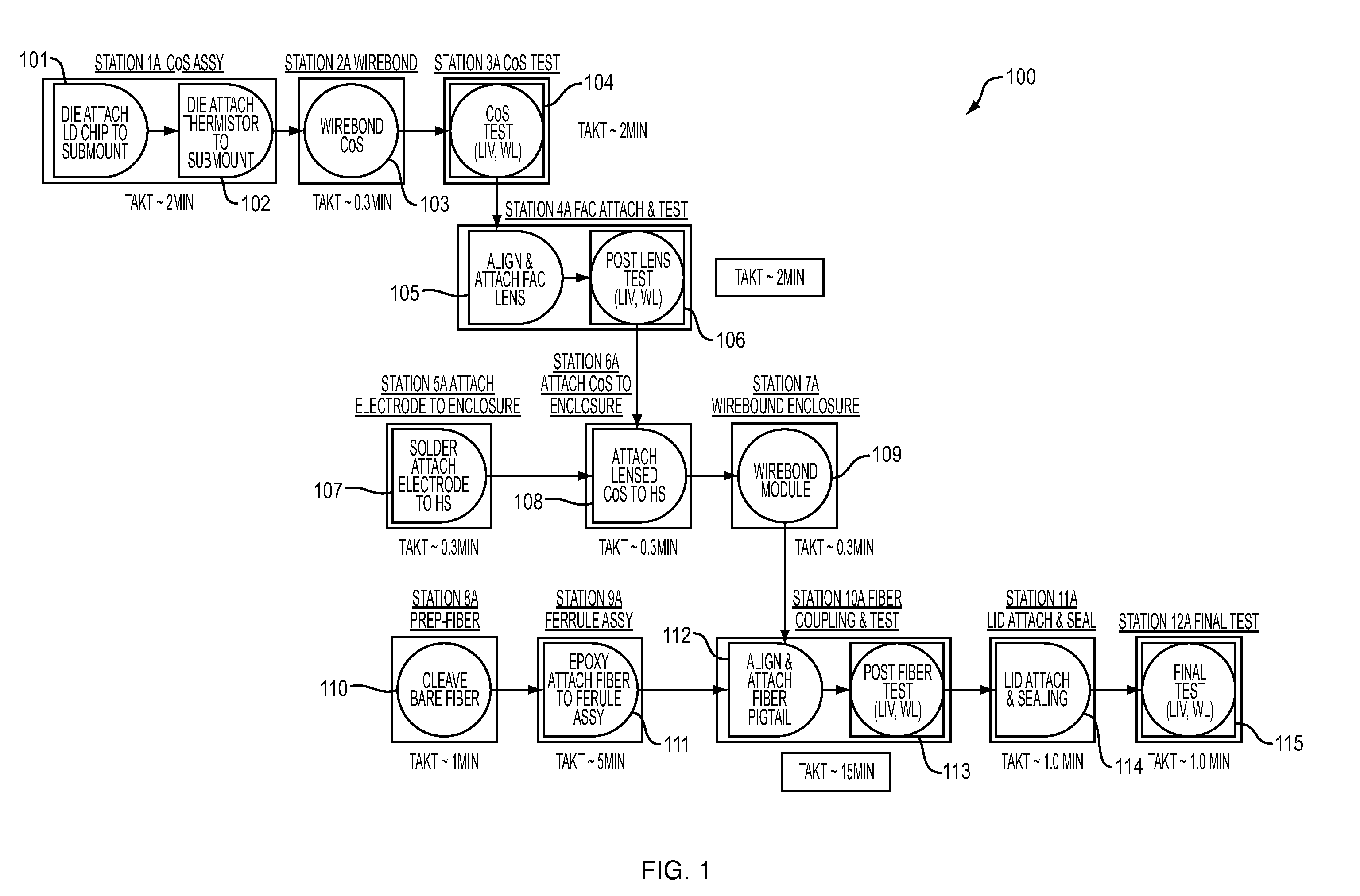
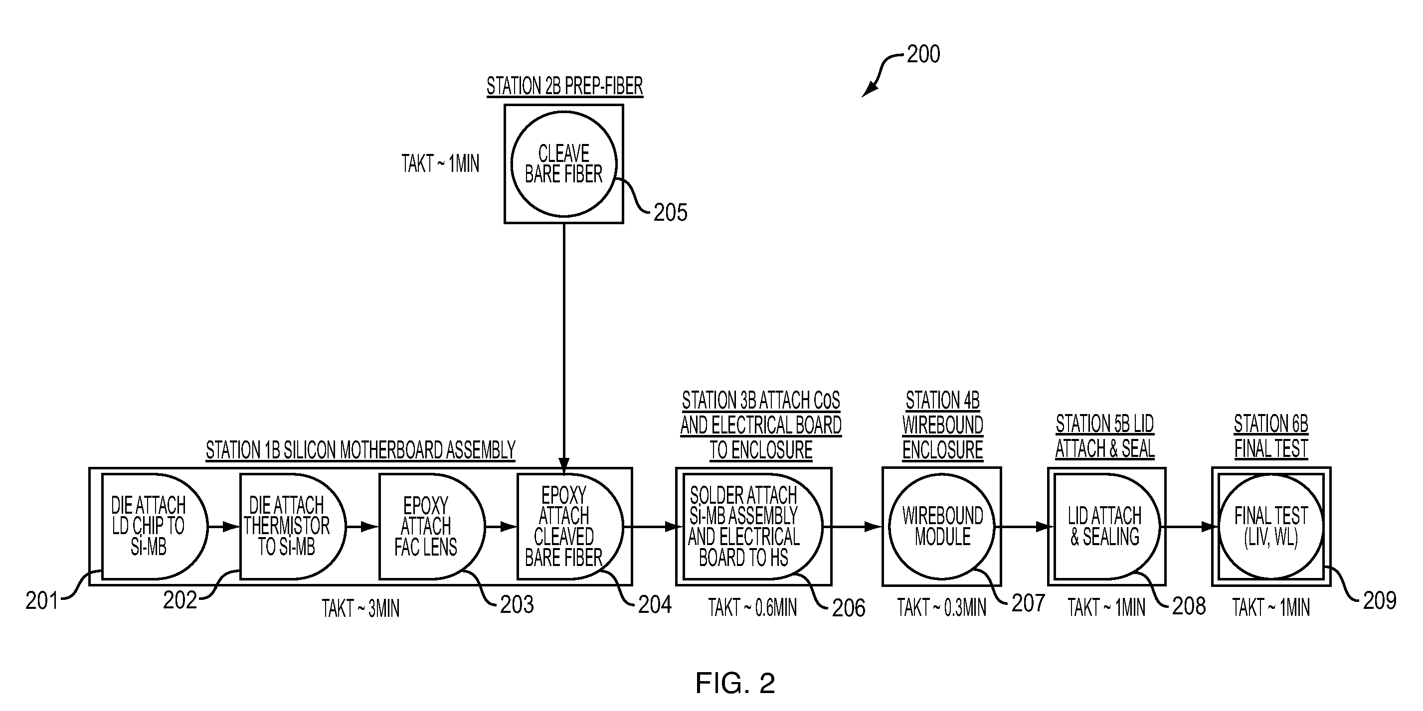
[0063]The ability to achieve a lower cost photonics module, relative to the cost of currently available photonics module(s), relies at least in part on a design that reduces the number of component parts that make up a photonics module. Alternatively or in addition, the ability to achieve a reduced cost photonic module relative to currently available photonics module(s) relies on a design that reduces the number of manufacturing steps, has a reduced amount of time required for manufacture of the photonics module (e.g., a reduced takt time), and / or a reduced amount of manufacturing equipment required to produce the module. In particular, the ability to achieve a reduced cost photonic module is enabled by one or more of the elimination of active alignment for the FAC lens and / or the optical fiber, a reduced number of component parts and a reduced number of manufacturing steps which achieve the same or better performance compared to currently available photonic modules which in one exe...


PUM

PropertyMeasurementUnit
thicknessaaaaaaaaaa
temperatureaaaaaaaaaa
thicknessaaaaaaaaaa

Abstract

An improved photonics module includes a Silicon motherboard having a plurality of v-grooves that collimate and optically align a laser diode emission is held within an enclosure that includes two or more positioning portions that locate and guide the Silicon motherboard in the desired position within the enclosure. The enclosure acts as a heat sink that provides stability and aids in wicking Silicon motherboard mounting material such damage to the Silicon motherboard by the mounting material is avoided. Methods of making the improved photonics module are also disclosed.

Description

BACKGROUND[0001]Photonics modules can include an optical component (e.g., an optical fiber and / or an optical lens) that is aligned with a photonic device. Currently, photonics modules having relatively high optical power (e.g., greater than 1 W) and relatively lower optical coupling loss (e.g., less than about 15% optical coupling loss) take a relatively long time to manufacture, require operator skill, and require operator intervention and / or high cost equipment to manufacture, and are, accordingly, relatively costly to manufacture. As a result, currently available photonics modules are employed in relatively higher cost end user applications (e.g., end user applications that are targeted for a professional practitioner rather than an end user such as a consumer). It is desirable to design a photonics module that is suitable for application in a device having a lower price point relative to current devices that incorporate photonics module(s).[0002]The generation of a high optical ...

Claims


Application Information

Patent Timeline
Patent Type & Authority Applications(United States)
IPC IPC(8): G02B6/32B23P11/00
CPCH01S5/02252H01S5/02272H01S5/02284Y10T29/49826H05K1/141H05K2201/10121H05K1/0274H01L2224/48091H01L2224/45144H01S5/02326H01S5/0237H01S5/02251H01L2924/00014H01L2924/00
Inventor WILSON, STEWART W.
Owner PALOMAR MEDICAL TECH
Why Eureka
Try Eureka