Charged particle beam device

a charge particle and beam technology, applied in the field of charge particle beam devices, can solve the problems of general difficulty in setting a pattern to be measured in the region of high magnification images, and achieve the effect of reducing measurement reproducibility and matching tools

Active Publication Date: 2012-05-03
HITACHI HIGH-TECH CORP
View PDF3 Cites 16 Cited by
  • Summary
  • Abstract
  • Description
  • Claims
  • Application Information

AI Technical Summary

Benefits of technology

[0015]According to the present invention, varying beam diameters attributed to image shift are compensated for and, thus, a decrease in measurement reproducibility as well as tool to tool matching induced by the varying beam diameters are improved.

Problems solved by technology

The reason why, after an image is captured at a low magnification, an image shift is performed and an image is captured again at a high magnification, without starting with capturing an image at a high magnification, is that it is generally hard to set a pattern to be measured covered in the region of a high magnification image due to insufficient precision of stopping the stage in place.
In addition to requirements in terms of individual tool reproducibility of measurement for CD SEMs, existing heretofore, it becomes a significant challenge to reduce a difference between dimensions measured by respective devices (tool to tool matching), because a plurality of CD SEMs are often used together in view of a relationship between the processing capacity of a single CD SEM and the amount of semiconductor production.

Method used


Image

  • Charged particle beam device
  • Charged particle beam device
  • Charged particle beam device

Examples


embodiment 1

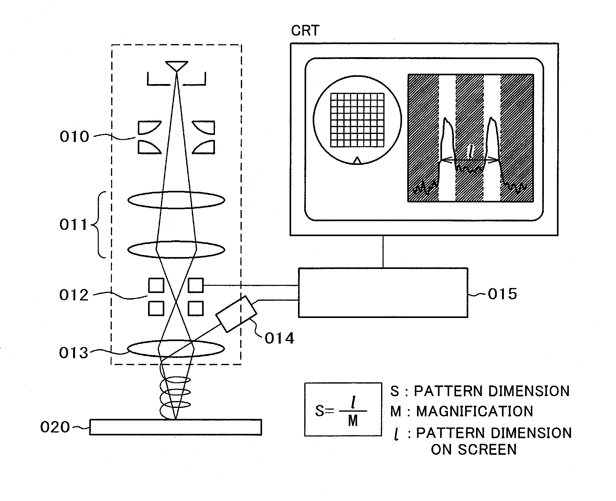
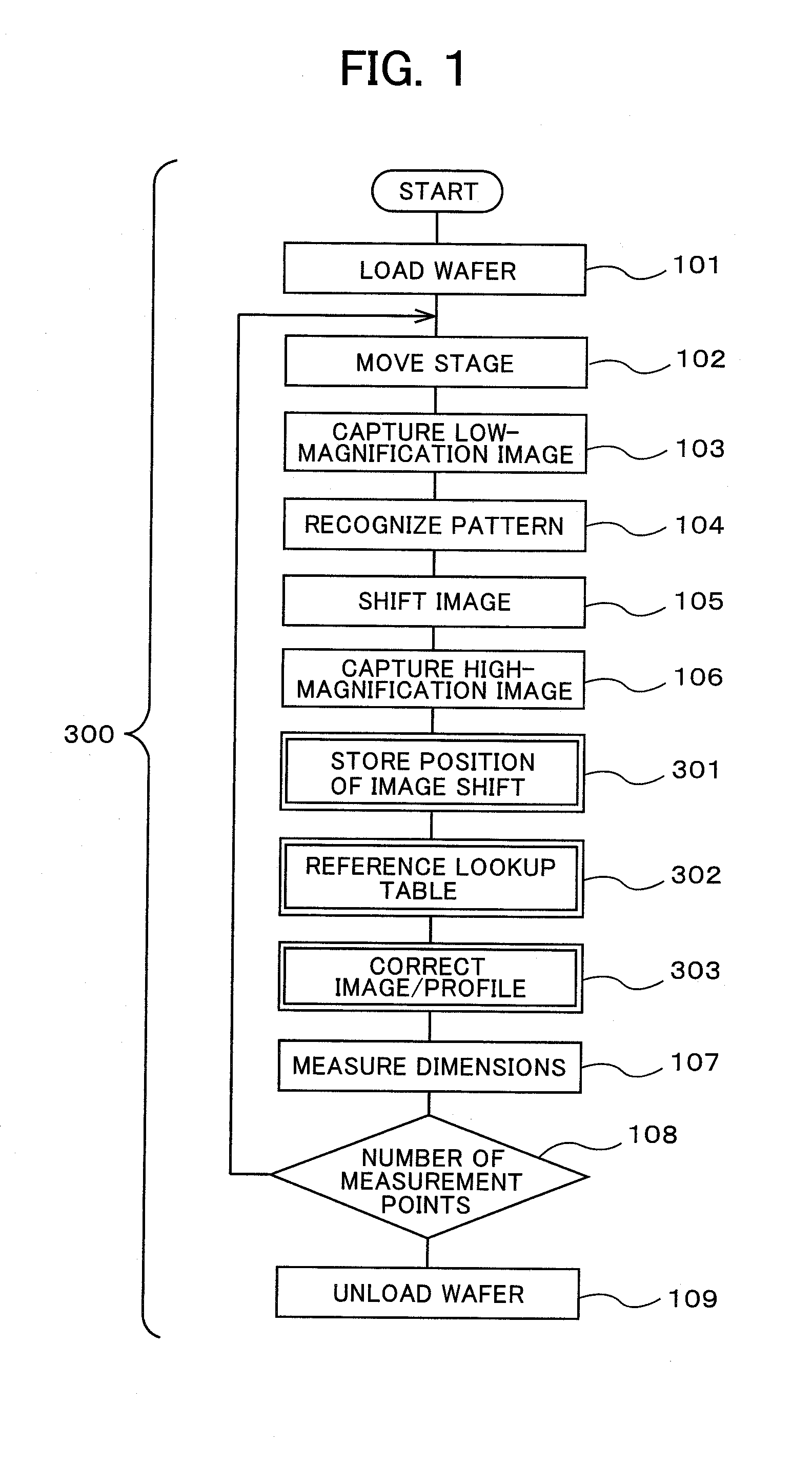
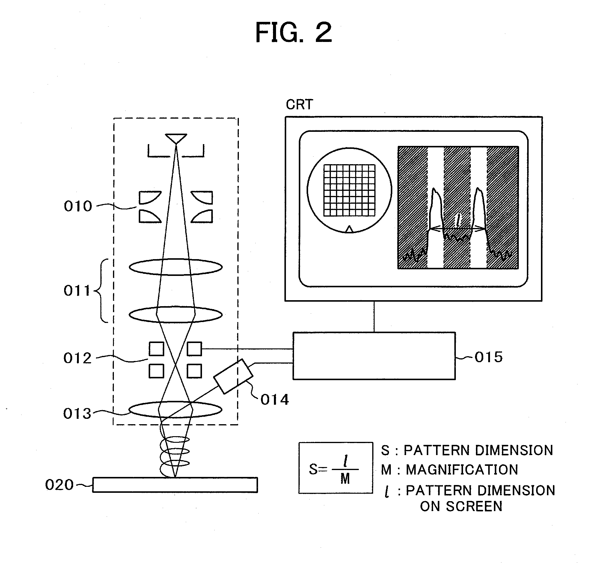
[0040]FIG. 1 illustrates a flow of dimension measurement in a charged particle beam device pertaining to the present invention. The steps of loading a wafer (step 101), moving the stage (step 102), capturing an image at a low magnification (step 103), pattern recognition (step 104), image shift (step 105), and capturing an image at a high magnification (step 106) are as described in the Background Art section.

[0041]In the present invention, a position of image shift (dx, dy) when capturing an image at a high magnification is stored (step 301), reference is made to a lookup table having a correlation between an image shift position and an image or profile correction coefficient stored therein (step 302), and a image or profile correction is performed (step 303). Then, dimension measurement is performed using the corrected image or profile (step 107).

[0042]How to create the lookup table used in step 302 and how to make correction in step 303 are detailed below. FIG. 6 illustrates a fl...

embodiment 2

[0064]While the first embodiment features evaluating correction coefficients for profile or image correction, amounts of change for dimension values measured at each image shift position may be determined beforehand and results may be registered into a lookup table. The structure of such a lookup table is shown in FIG. 15. Offset values to adjust dimension measurement results are described in the lookup table.

[0065]Lookup tables in the foregoing first embodiment are registered for each imaging condition. However, lookup tables need to be registered for each imaging condition (acceleration voltage, beam divergence angle, etc.) and for each pattern to be measured, because the amounts of change for dimension measurement values differ depending on the pattern to be measured. In a case that the number of types of patterns to be measured is small, this embodiment is beneficial.

embodiment 3

[0066]While, in the first embodiment, a relationship between image shift positions and varying beam diameters is obtained by actual measurement in the flow shown in FIG. 6, beam diameters at all image shift positions may be calculated by a SEM optics simulator and results may be converted to correction coefficients which then may be registered into a lookup table.

[0067]More specifically, in this embodiment, given that the beam diameter at a given image shift position is bwn in terms of a Gauss function and the maximum beam diameter in the sphere of image shifting is bwmax in terms of a Gauss function, a correction coefficient σn associated with each image shift position is calculated by σn=(bwmax2−bwn2)1 / 2 Results of this calculation are registered into a lookup table as shown in FIG. 12, as is the case for the first embodiment, and profile or image correction is performed by the method illustrated in FIG. 14(b), as is the case for the first embodiment.


PUM


Abstract

A charged particle beam device enabling prevention of degradation of reproducibility of measurement caused by an increase of the beam diameter attributed to an image shift and having a function of dealing with device-to-device variation. The charged particle beam device is used for measuring the dimensions of a pattern on a specimen using a line profile obtained by detecting secondary charged particles emitted from the specimen when the specimen is scanned with a primary charged particle beam converged on the specimen. A lookup table in which the position of image shift and the variation of the beam diameter are associated is prepared in advance by actual measurement or calculation and registered. When the dimensions are measured, image processing is carried out so as to correct the line profile for the variation of the beam diameter while the lookup table is referenced, and thereby the situation where the beam diameter is effectively equal is produced irrespective of the position of the image shift. Whit this, measurement by the charged particle beam excellent reproducibility can be carried out.

Description

TECHNICAL FIELD[0001]The present invention relates to a charged particle beam device for measuring microscopic dimensions and, in particular, to such device for measuring pattern dimensions in semiconductor devices.BACKGROUND ART[0002]As described in Non-Patent Document 1, a critical dimension SEM which is a type of Scanning Electron Microscope (SEM) that is specialized for semiconductors is used for management of pattern dimensions in a semiconductor production process. The principle of the critical dimension SEM is shown in FIG. 2. A primary electron beam emitted from an electron gun 010 is narrowed and converged by convergence lenses 011 and a specimen is two-dimensionally scanned with the electron beam through a deflector 012 (scanning coil).[0003]A detector 014 captures secondary electrons emitted from the specimen 020 as a result of irradiating the specimen 020 with the electron beam focused on the surface of the specimen 020 by an objective lens 013, with the result that an e...

Claims


Application Information

Patent Timeline
Patent Type & Authority Applications(United States)
IPC IPC(8): H01J37/26
CPCG01B2210/56H01J37/244H01J37/28H01J2237/2826H01J2237/24578H01J2237/24592H01J2237/2817H01J37/3045G01B15/00H01J37/22
Inventor SHISHIDO, CHIEMIYAMOTO, ATSUSHIIWASAKI, MAYUKANISHIURA, TOMOFUMIKOTAKI, GO
Owner HITACHI HIGH-TECH CORP
Why Eureka
Try Eureka