Thin film transistor and method for producing the same

a thin film transistor and film technology, applied in transistors, semiconductor devices, electrical equipment, etc., can solve the problems of affecting the operation speed of the driver circuit, damaging the amorphous silicon tft, etc., and achieves high dielectric breakdown voltage, high blocking effect, and suppressed threshold voltage increase in shift amount

Inactive Publication Date: 2012-05-03
SHARP KK
View PDF0 Cites 8 Cited by
  • Summary
  • Abstract
  • Description
  • Claims
  • Application Information

AI Technical Summary

Benefits of technology

[0022]According to the first aspect of the present invention, in a thin film transistor having a channel layer that is made of microcrystalline silicon, a gate insulating film is a film formed by laminating a first silicon nitride film having a nitrogen concentration of 6×10²¹ atoms / cc or less and a second silicon nitride film having a nitrogen concentration higher than 6×10²¹ atoms / cc. The second silicon nitride film has a high blocking effect against mobile ions entering from an insulating substrate, making the mobile ions less likely to be stored in an interface with the channel layer. Therefore, even when the thin film transistor is operated under a high temperature environment, an increase in shift amount of the threshold voltage can be suppressed. Furthermore, since the first silicon nitride film is included in the gate insulating film, the gate insulating film has a high dielectric breakdown voltage.
[0023]According to the second aspect of the present invention, the second silicon nitride film having a high nitrogen concentration is formed so as to be in contact with the channel layer. Therefore, mobile ions entering from the insulating substrate can be prevented from entering the interface between the channel layer and the gate electrode and from being stored in the interface. As a result, the shift amount of the threshold voltage of the thin film transistor is suppressed.
[0024]According to the third aspect of the present invention, the nitrogen concentrations in the first and second silicon nitride films are constant inside the respective films. Therefore, the first and second silicon nitride films can be formed in a simple manner.
[0025]According to the fourth aspect of the present invention, in the second silicon nitride film, the nitrogen concentration in an end on a side of the channel layer is higher than the nitrogen concentration on a side of the insulating substrate, thereby making the mobile ions entering from the insulating substrate less likely to be stored in the interface between the channel layer and the gate insulating film. Therefore, the shift amount of the threshold voltage of the thin film transistor can be suppressed. Because the nitrogen concentration inside the second silicon nitride film on a side of the first silicon nitride film is low, the dielectric breakdown voltage becomes high not only in the first silicon nitride film, but also in a portion of the second silicon nitride film. Thus, the dielectric breakdown voltage of the overall gate insulating film becomes higher.
[0026]According to the fifth aspect of the present invention, the thickness of the first silicon nitride film is 3 / 7 to 7 / 3 times the film thickness of the second silicon nitride film. Therefore, the blocking effect against mobile ions can be improved and the dielectric breakdown voltage can be increased at the same time.
[0027]According to the sixth aspect of the present invention, the oxygen concentration in an interface between the channel layer and either the first or second silicon nitride film that is in contact with the channel layer is set at 1×10²¹ atoms / cc or less to decrease the interface state density. This way, the OFF currents of the thin film transistor can be decreased significantly.

Problems solved by technology

When a driver circuit of such a liquid crystal display device is formed of thin film transistors (Thin Film Transistors, hereinafter referred to as “TFTs”) made of amorphous silicon, there is a problem that the operation speed of the driver circuit slows down because the mobility of the amorphous silicon is low.
In addition, when a TFT having a channel layer that is made of amorphous silicon (hereinafter referred to as an “amorphous silicon TFT) undergoes a gate bias stress test in which a constant voltage is applied to its gate electrode for a long time, there is another problem that the threshold voltage shifts significantly, damaging the amorphous silicon TFT.

Method used


Image

  • Thin film transistor and method for producing the same
  • Thin film transistor and method for producing the same
  • Thin film transistor and method for producing the same

Examples


modification examples

6. Modification Examples

6.1 First Modification Examples

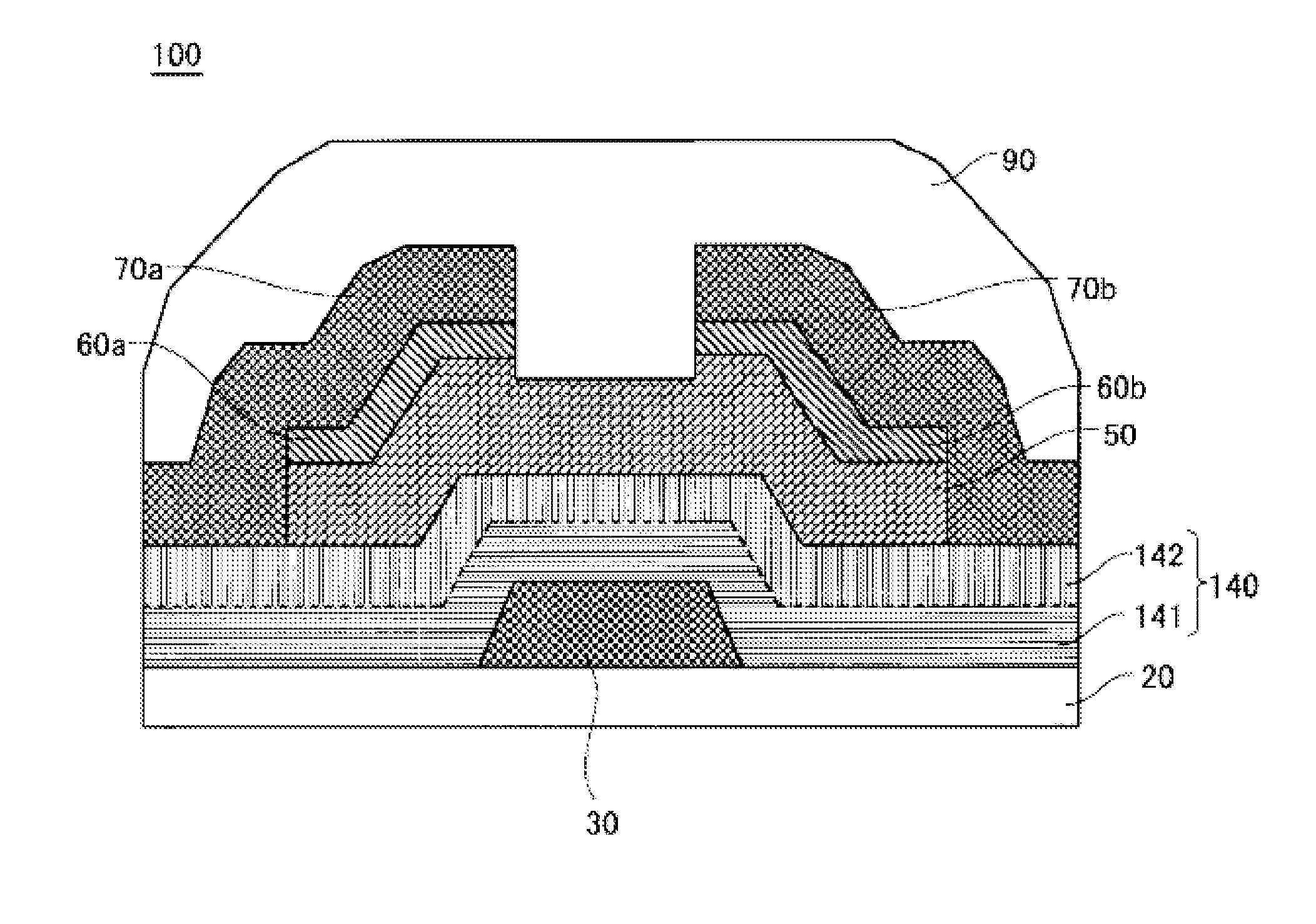
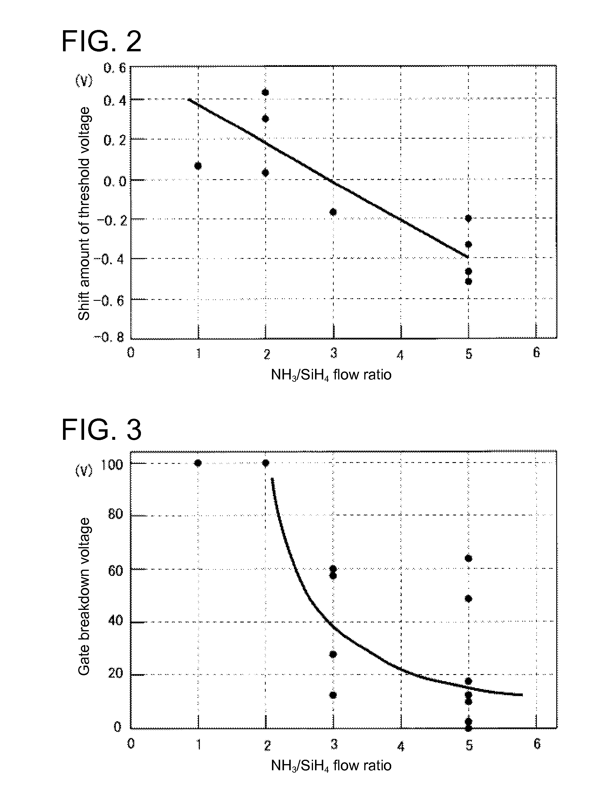
[0095]In the microcrystalline silicon TFT 100 of the above-mentioned embodiment, the nitrogen concentration was set to be constant inside the first and second silicon nitride films 141 and 142, respectively. However, as described above, it is sufficient if the nitrogen concentration inside the first silicon nitride film 141 is 6×10²¹ atoms / cc or less and the nitrogen concentration inside the second silicon nitride film 142 is higher than 6×10²¹ atoms / cc. As long as these conditions are met, the nitrogen concentration may not be constant inside the first and second silicon nitride films 141 and 142, respectively. Thus, cases in which the nitrogen concentration varies inside the first and second silicon nitride films 141 and 142, respectively, are described below.

[0096]FIG. 13(A) is a drawing showing a modification example of changes in the nitrogen concentration when the second silicon nitride film 142 is laminated on the upper s...

second modification examples

6.2 Second Modification Examples

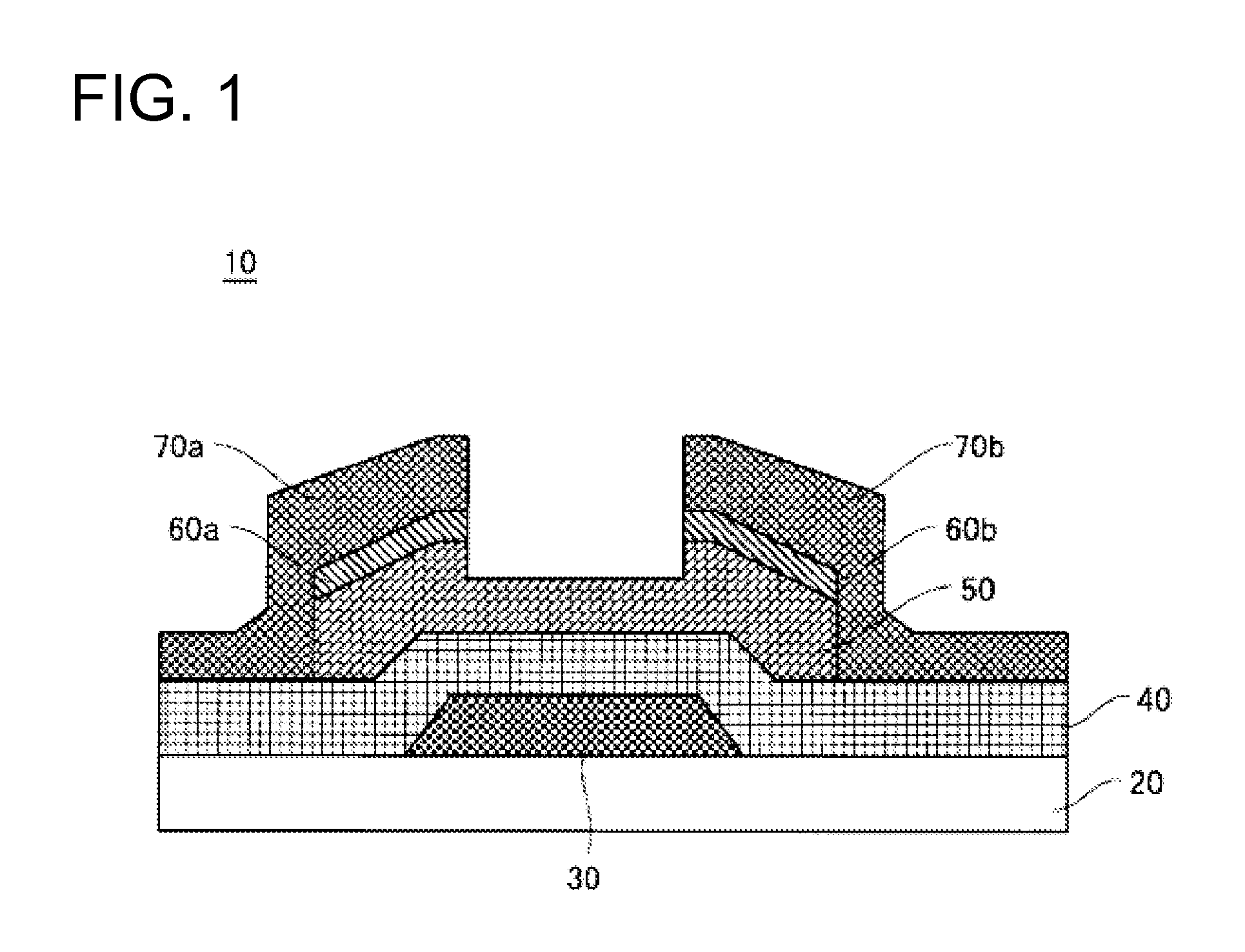
[0105]In the above-mentioned embodiment, the bottom gate type microcrystalline silicon TFTs 100 were described. However, even in a top gate type microcrystalline silicon TFT, effects similar to those of the bottom gate type microcrystalline silicon TFT 100 can be obtained by using a film formed by laminating the above-mentioned first and second silicon nitride films 141 and 142 as a gate insulating film. Furthermore, by performing either a hydrogen plasma treatment or a hydrofluoric acid treatment on a surface of either the first or second silicon nitride film that forms an interface with a channel layer, OFF currents can be reduced in a manner similar to the bottom gate type microcrystalline silicon TFT 100.

[0106]The bottom gate type microcrystalline silicon TFT and the top gate type microcrystalline silicon TFT are not limited to an n-channel type, and may be a p-channel type TFT.


PUM


Abstract

An object of the present invention is to provide a thin film transistor having a gate insulating film for suppressing a shift amount of a threshold voltage generated by use under a high temperature environment. In a thin film transistor having a channel layer made of microcrystalline silicon, a gate insulating film 140 is a film obtained by laminating a first silicon nitride film 141 having a nitrogen concentration of 6×10²¹ atoms/cc or less and a second silicon nitride film 142 having a nitrogen concentration higher than 6×10²¹ atoms/cc. Therefore, the second silicon nitride film 142 increases the blocking effect against mobile ions entering from a glass substrate 20 to make the mobile ions less likely to be stored in an interface with a channel layer 50. The first silicon nitride film 141 increases the dielectric breakdown voltage of the gate insulating film 140.

Description

TECHNICAL FIELD[0001]The present invention relates to a thin film transistor and a manufacturing method thereof, and particularly, to a thin film transistor suited for a driver circuit of an active matrix type display device and a manufacturing method thereof.BACKGROUND ART[0002]In recent years, a liquid crystal display device that is called a “monolithic driver type liquid crystal display device” in which driver circuits, such as a gate driver, a source driver, and the like, are integrally formed in a frame section of a liquid crystal panel has been manufactured.[0003]When a driver circuit of such a liquid crystal display device is formed of thin film transistors (Thin Film Transistors, hereinafter referred to as “TFTs”) made of amorphous silicon, there is a problem that the operation speed of the driver circuit slows down because the mobility of the amorphous silicon is low. In addition, when a TFT having a channel layer that is made of amorphous silicon (hereinafter referred to a...

Claims


Application Information

Patent Timeline
Patent Type & Authority Applications(United States)
IPC IPC(8): H01L29/786H01L29/04H01L21/336
CPCH01L21/0217H01L21/022H01L29/78678H01L29/4908H01L29/66765H01L29/04
Inventor KOHNO, AKIHIKOMORIGUCHI, MASAOSAITOH, YUHICHI
Owner SHARP KK
Why Eureka
Try Eureka