
Eureka
For R&D, Eureka makes reading and utilizing patents & technical documents easy.
Eureka AIR
Designed for self-driven R&D workflows. Generate viable solutions, solve complex R&D challenges, empower your innovation with AI.

Eureka Materials
Designed for material experts only. Revolutionize your material R&D, from search, analyze, to developing new materials.

TechResearch
Generate reliable direction feasibility study reports for your R&D in just a few steps.

TechSeek
Discover and master advanced knowledge NOW. Basics, ideas, possibilities, all at once.

TechMind
As an expert in R&D Theories, TechMind can generates customized viable solutions instantly.

TechRisk
Analyze your overall solution with one click, know your potential R&D risks in advance.

TechMonitor
Get weekly tech updates, stay abreast of the latest tech innovations and key insights.
Semiconductor device
- Summary
- Abstract
- Description
- Claims
- Application Information
AI Technical Summary
Problems solved by technology
Method used
Image

Examples
first embodiment
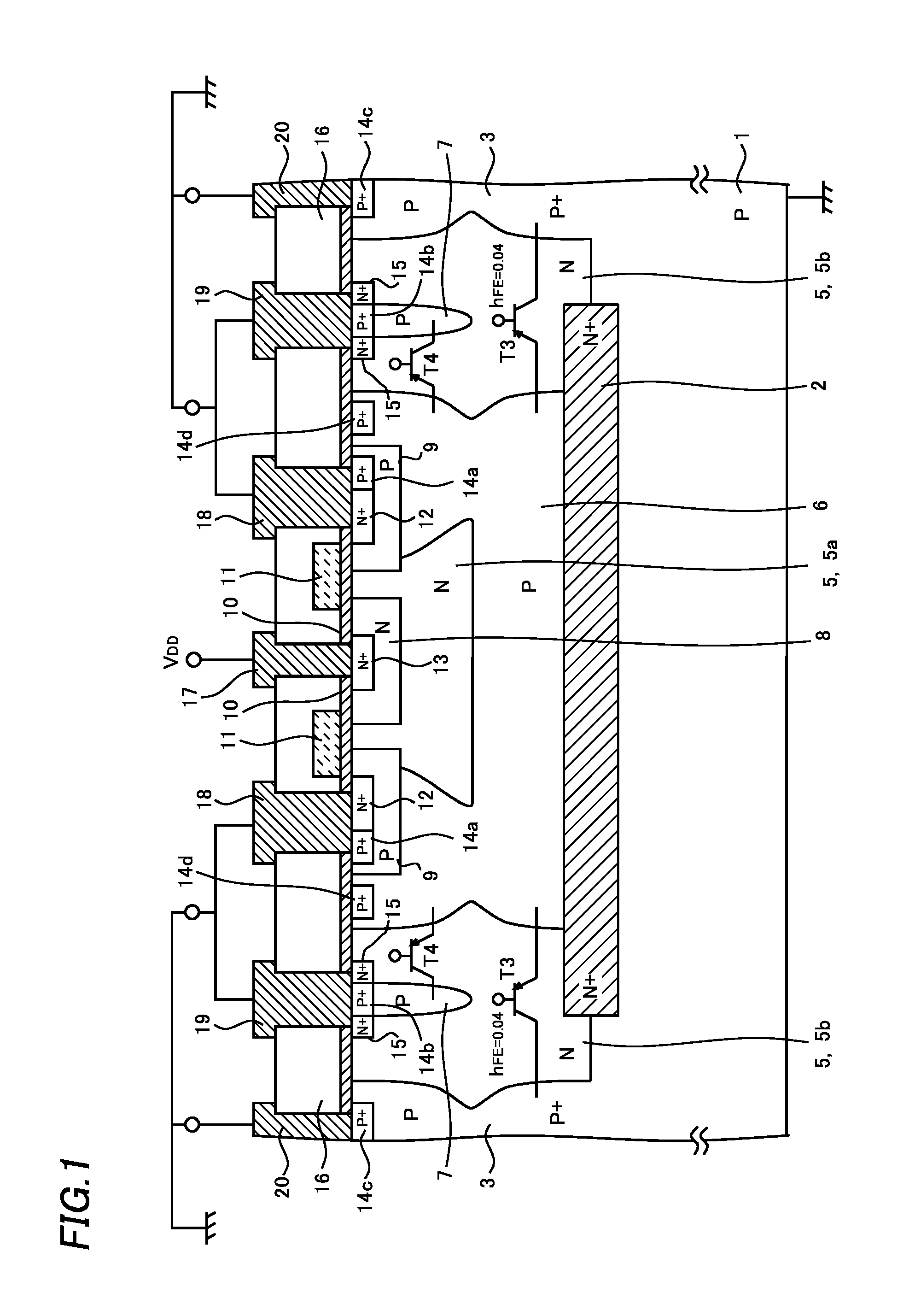
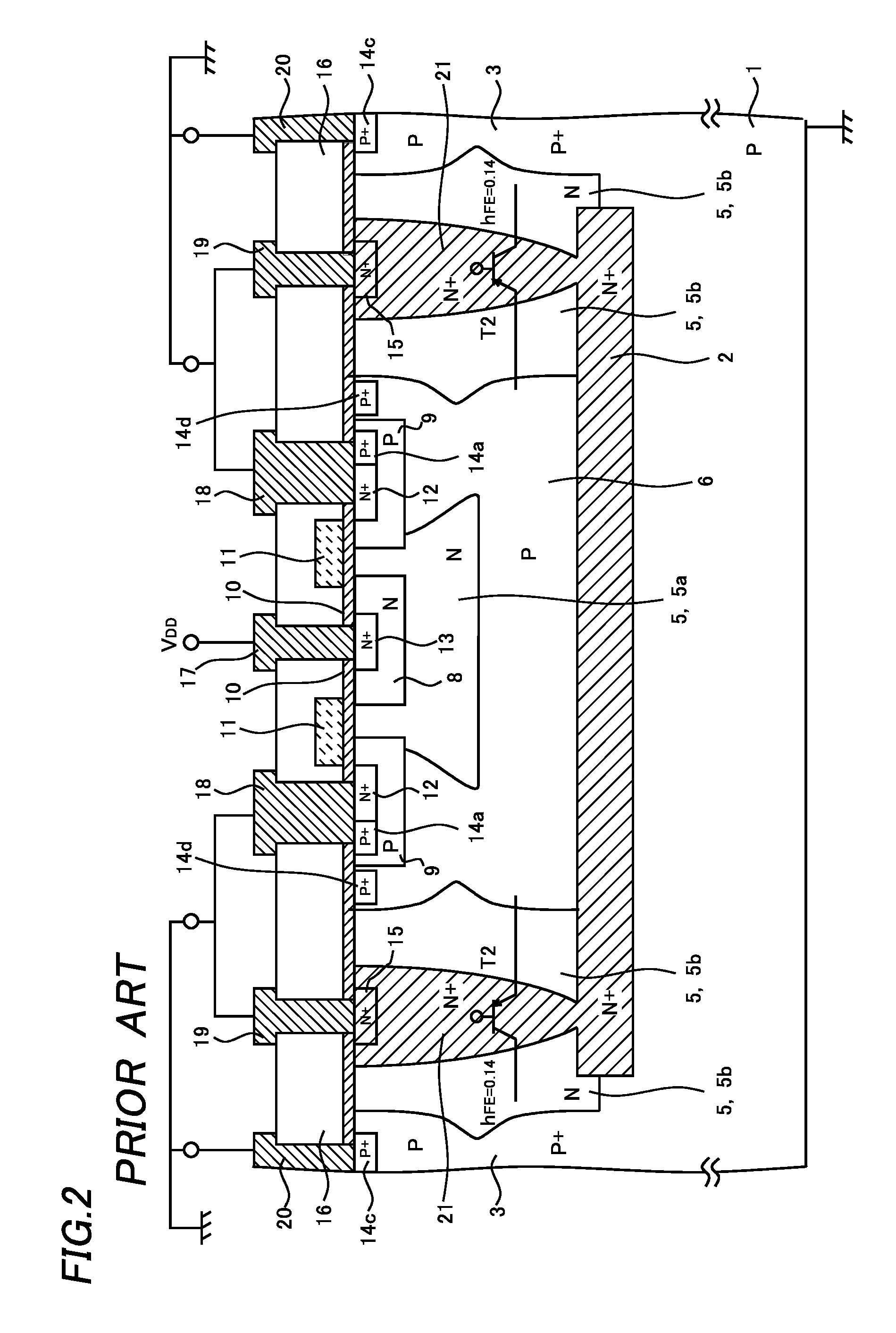
[0030]A drain isolated type LDMOS transistor of a first embodiment will be described referring to FIGS. 1 to 5B in comparison with a drain isolated type LDMOS transistor having a conventional structure.
[0031]In the drain isolated type LDMOS transistor of the first embodiment, a source region including an N+ type source layer 12 is formed symmetrically with respect to a drain region including an N+ type drain 13, as shown in FIG. 1. FIG. 1 is a cross-sectional view showing the drain isolated type LDMOS transistor and a method of manufacturing the same of the first embodiment. FIG. 11A is a schematic plan view of this LDMOS transistor, and FIG. 1 is a cross-sectional view thereof along line A-A. An N type epitaxial layer 5 is formed on a P type semiconductor substrate 1, being divided into a plurality of regions by P type element isolation layers 3. An N+ type buried layer 2 is formed in a boundary region between one of the N type epitaxial layers 5 divided by the P type element isola...
second embodiment
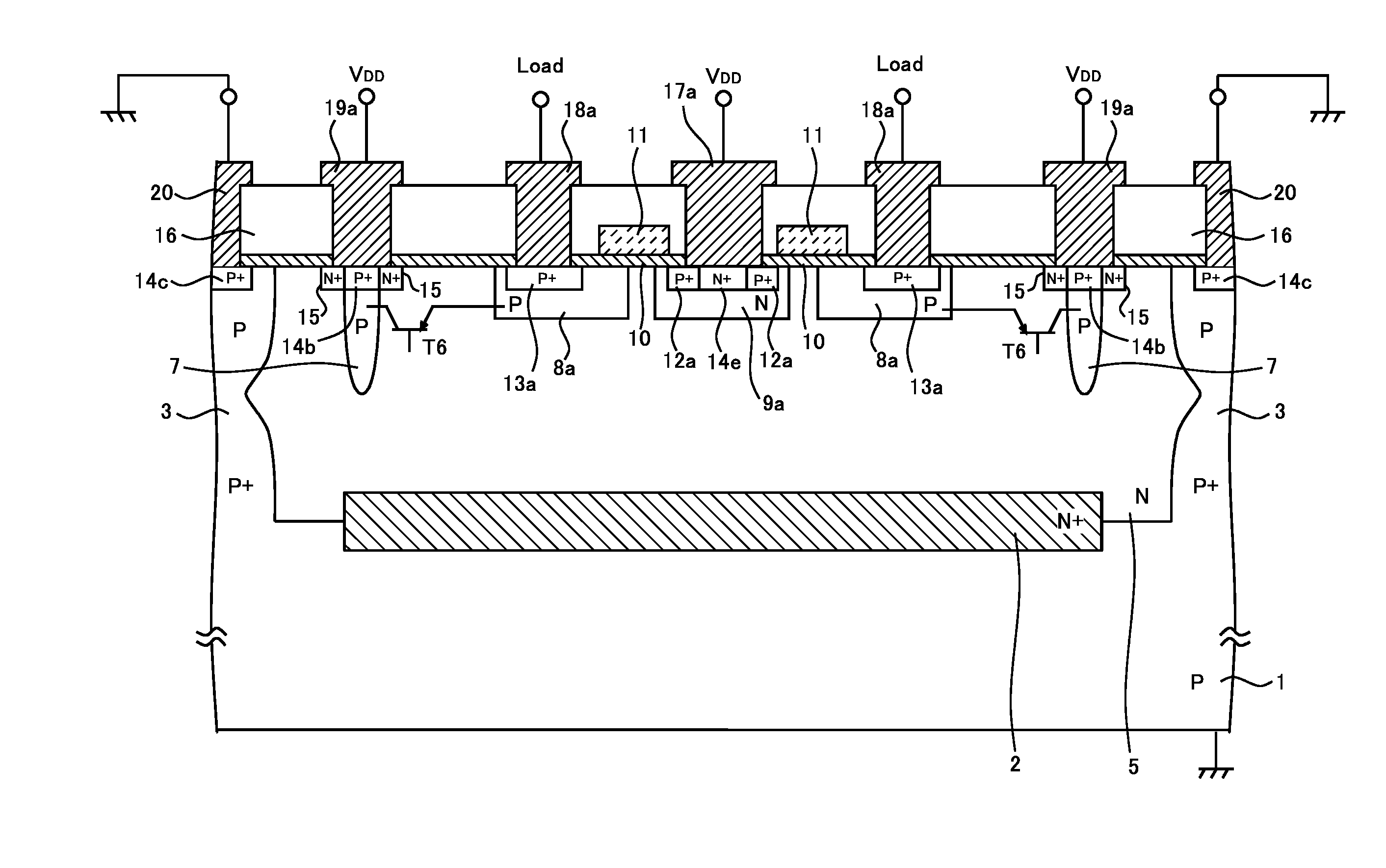
[0079]When a large positive voltage is applied to a drain electrode 18a of the P channel type ordinary type LDMOS transistor like in the second embodiment, the PN junction between the N type epitaxial layer 5 and a P type drift layer 8a is forward-biased. Therefore, a surge current flows from a source electrode 17a to the power supply line VDD through the N type body layer 9a and the N+ type contact layer 14e.
[0080]Furthermore, a parasitic PNP bipolar transistor T6 that uses the P type drift layer 8a as the emitter, the N type epitaxial layer 5 as the base, and the P type collector layer 7 as the collector also turns to the on-state operation state, and a surge current flows into the power supply line VDD through the collector electrode 19a.
[0081]At this time, like in the second embodiment, a parasitic PNP bipolar transistor (not shown) that uses the P type drift layer 8a as the emitter, the N type epitaxial layer 5 as the base, and the P type semiconductor substrate 1 as the coll...
PUM
 Abstract
Description
Claims
Application Information
 - R&D Engineer
- R&D Manager
- IP Professional
- Industry Leading Data Capabilities
- Powerful AI technology
- Patent DNA Extraction
Browse by: Latest US Patents, China's latest patents, Technical Efficacy Thesaurus, Application Domain, Technology Topic, Popular Technical Reports.
© 2024 PatSnap. All rights reserved.Legal|Privacy policy|Modern Slavery Act Transparency Statement|Sitemap|About US| Contact US: help@patsnap.com