Power semiconductor module

a technology of semiconductor modules and semiconductor devices, applied in the direction of power conversion systems, semiconductor devices, ac-dc conversion, etc., to achieve the effects of reducing electromagnetic noise, facilitating reducing mutual inductance, and reducing manufacturing costs

Active Publication Date: 2012-05-17
FUJI ELECTRIC CO LTD
View PDF3 Cites 32 Cited by
  • Summary
  • Abstract
  • Description
  • Claims
  • Application Information

AI Technical Summary

Benefits of technology

[0026]In view of the foregoing, it would be desirable to obviate the problems described above. It would be also desirable to provide, with low manufacturing costs, a power semiconductor module that facilitates reducing the mutual inductance therein, reducing the electromagnetic noises introduced into the control terminals thereof, and attaching external wirings to the terminals thereof simply and easily.

Problems solved by technology

However, Patent Document 1 does not describe any thing on the technique for reducing the wiring inductance between the IGBT's in the module.

Method used


Image

  • Power semiconductor module
  • Power semiconductor module
  • Power semiconductor module

Examples


first embodiment

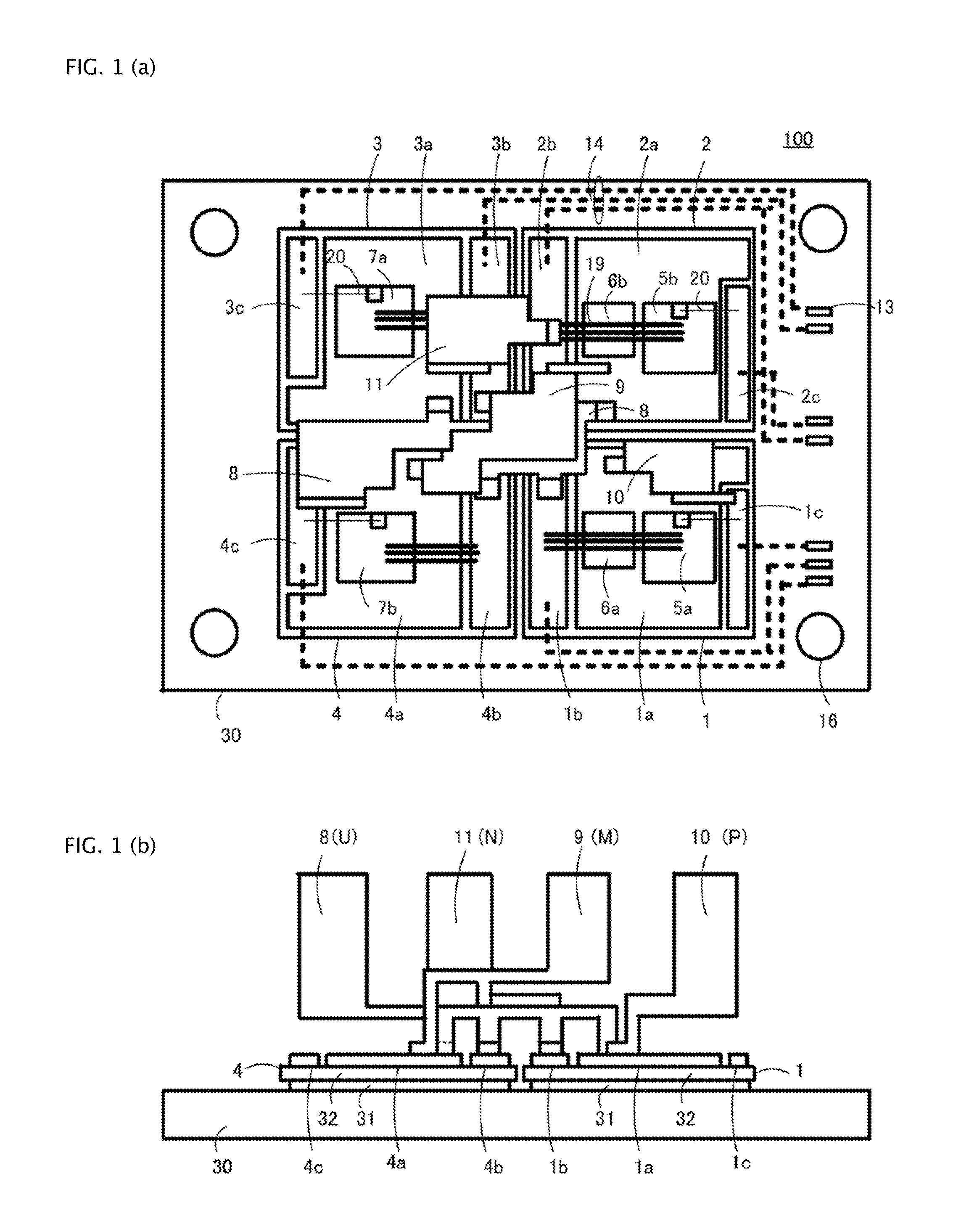
[0075]FIG. 1(a) is the top plan view of a power semiconductor module according to a first embodiment of the invention. FIG. 1(b) is the side plan view of the power semiconductor module according to the first embodiment. In FIG. 1(b), insulated-gate bipolar transistor chips (hereinafter referred to as “IGBT chips”) and freewheel diode chips (hereinafter referred to as “FWD chips”) are not shown for the convenience of descriptions.

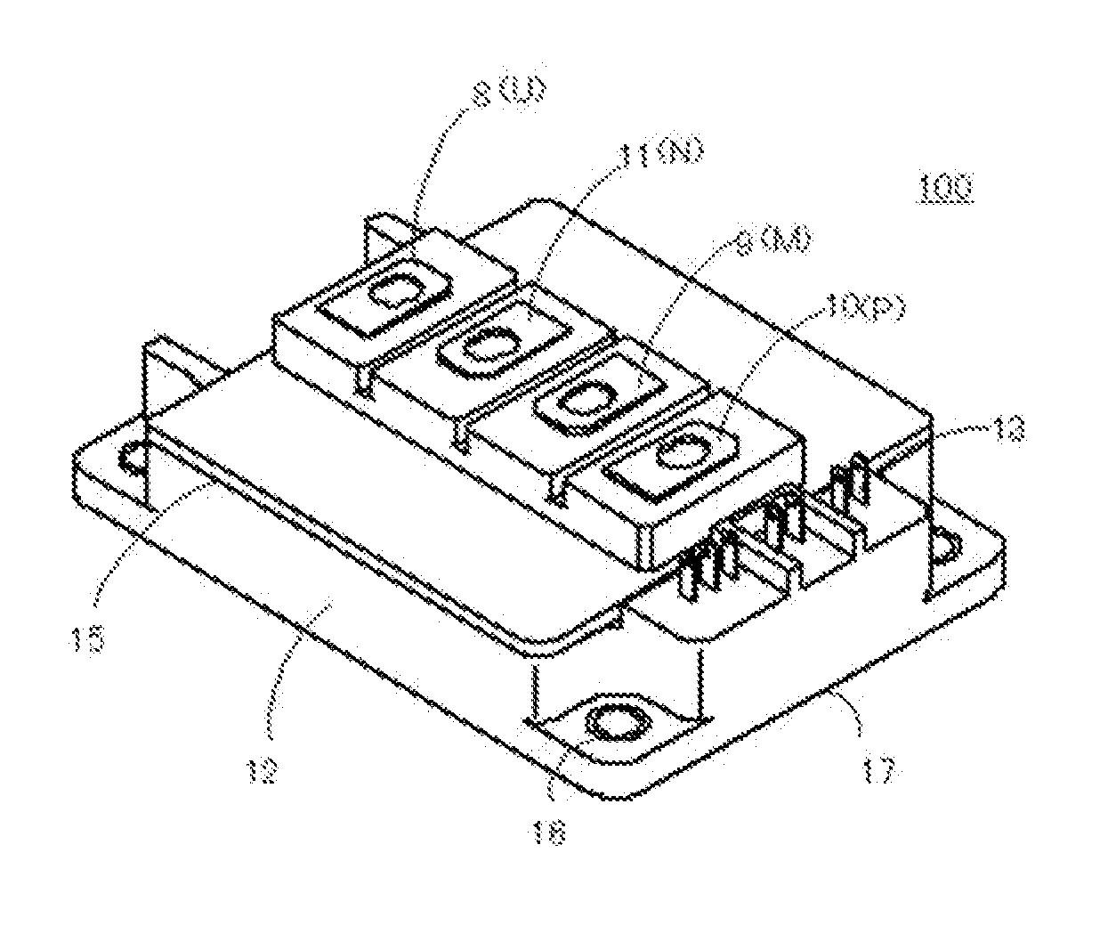
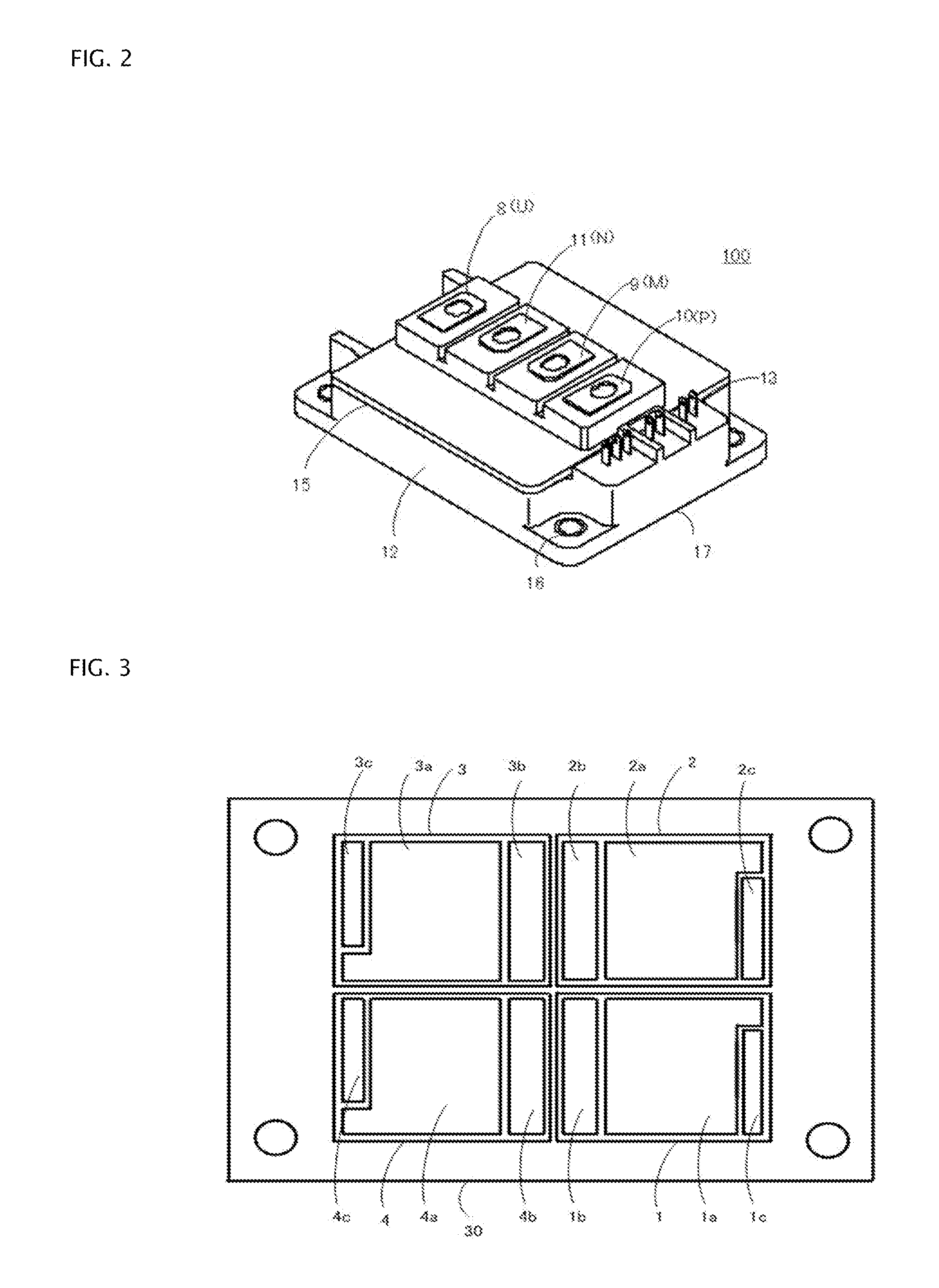
[0076]FIG. 2 is the isometric view of the power semiconductor module according to the first embodiment showing the external appearance thereof.

[0077]FIG. 3 is a top plan view showing a radiator plate and insulated substrates, each including an electrical-conductor pattern formed thereon.

[0078]FIG. 4 is a top plan view showing chips fixed to the electrical-conductor patterns. FIG. 5 is a top plan view showing terminals fixed to the electrical-conductor patterns. FIG. 6(a) is the top plan view of a U-terminal. FIG. 6(b) is the side plan view of the U-terminal....

second embodiment

[0127]FIG. 14(a) is the top plan view of a power semiconductor module according to a second embodiment of the invention. FIG. 14(b) is the side plan view of the power semiconductor module according to the second embodiment. FIG. 15 is the top plan view of a case showing the terminal arrangement thereon. FIG. 16 is the top plan view of the power semiconductor module according to the second embodiment describing the current paths therein. FIG. 17 is the equivalent circuit diagram that considers the chip arrangement in FIG. 14(a).

[0128]Power semiconductor module 200 shown in FIGS. 14(a) and 14(b) is the same with power semiconductor module 100 shown in FIGS. 1(a) and 1(b) in that power semiconductor module 200 employs same insulated substrates 1, 2, 3, and 4; IGBT chips 5a and 5b; FWD chips 6a and 6b; and reverse blocking IGBT chips 7a and 7b. Power semiconductor module 200 is different from power semiconductor module 100 in that U-terminal 8 is shifted to the P-terminal 10 side and co...


PUM


Abstract

In a semiconductor module according to certain aspects the invention, a U-terminal and an M-terminal overlap each other in a manner to reduce inductance and to further to reduce the size of snubber capacitor. In certain aspects of the invention, a P-terminal, M-terminal, N-terminal, and U-terminal are arranged such that the U-terminal, through which currents flow in and out, is arranged farthest away from control electrodes to reduce the noises superposed to control electrodes, and the P-terminal, M-terminal, N-terminal, and U-terminal are aligned to facilitate attaching external connection bars thereto. A power semiconductor module according to aspects of the invention can facilitate reducing the wiring inductance inside and outside the module, reducing the electromagnetic noises introduced into the control terminals, and attaching the external wirings to the terminals thereof simply and easily.

Description

BACKGROUND OF THE INVENTION[0001]1. Field of the Invention[0002]Embodiments of the present invention relate to power semiconductor modules used in three-level inverters and resonance-type inverters.[0003]2. Description of Related Art[0004]FIG. 18 is the circuit diagram of a three-level inverter that converts a direct current (“DC”) to an alternating current (“AC”) using a conventional technique.[0005]The circuit configuration shown in FIG. 18 is disclosed in Japanese Unexamined Patent Application Publication No. 2008-193779, also referred to herein as “Patent Document 1.” DC power supplies 41 and 42 are connected in series to each other. In FIG. 18, positive electrode potential P, negative electrode potential N, and neutral point potential M are described. If one wants to configure the DC power supply from an AC power supply system, it is possible to configure the DC power supply using a diode rectifier and a large-capacity electrolytic capacitor, which are not shown.[0006]Series co...

Claims


Application Information

Patent Timeline
Patent Type & Authority Applications(United States)
IPC IPC(8): H01L29/739
CPCH01L24/49H01L25/072H01L2224/49175H02M7/487H01L29/7393H01L2924/01068H01L2924/13055H01L2924/1305H01L2924/30107H01L2924/01019H01L2924/00H01L2224/48137H01L2224/0603H01L2224/48227H01L2224/49111H01L2924/00014H01L24/48H01L2224/45099H01L2224/45015H01L2924/207
Inventor OKITA, SOUICHI
Owner FUJI ELECTRIC CO LTD
Why Eureka
Try Eureka