Wavelength-tunable laser system
a wavelength-tunable laser and laser system technology, applied in the direction of laser details, instruments, electrical equipment, etc., can solve the problems of high packaging cost, limited wavelength-tunable band, inaccurate wavelength tuning, etc., and achieve the effect of small size and high precision
- Summary
- Abstract
- Description
- Claims
- Application Information
AI Technical Summary
Benefits of technology
Problems solved by technology
Method used
Image
Examples
first exemplary embodiment
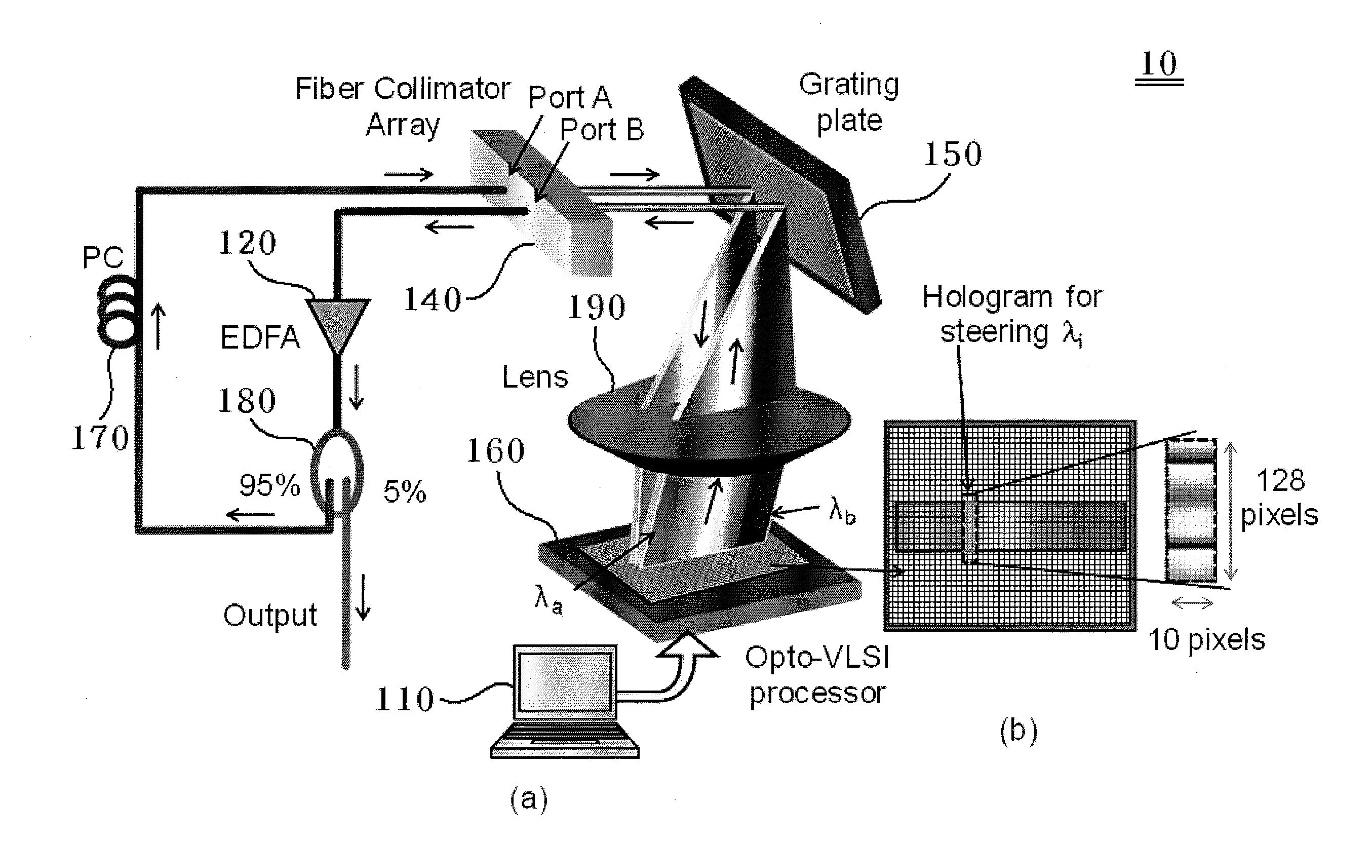
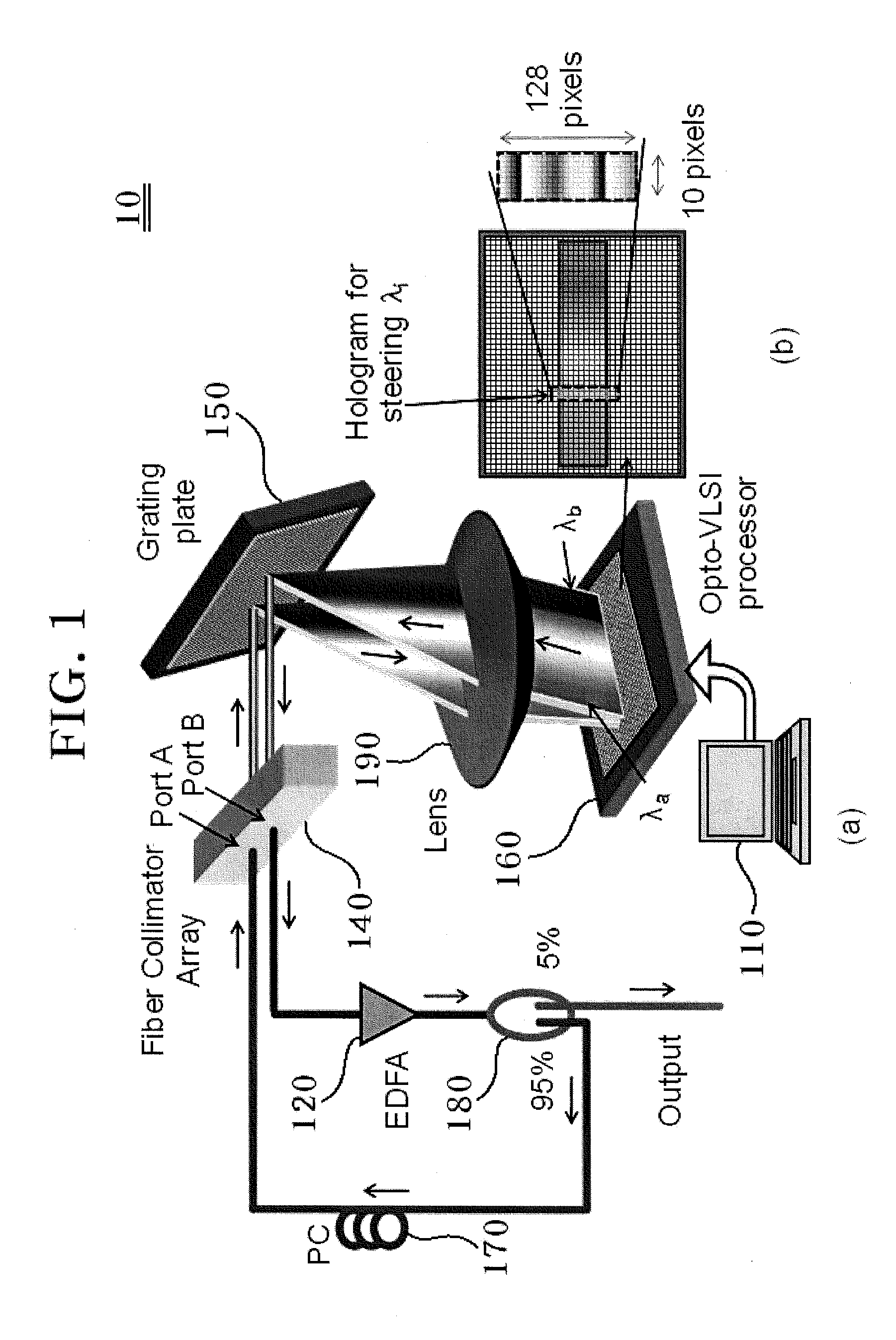
[0028]FIG. 1 is a schematic configuration diagram of a wavelength-tunable laser system according to a first exemplary embodiment of the present invention.
[0029]Referring to FIG. 1, the wavelength-tunable laser system 10 includes an optical spectrum analyzer 110, a polarization controller (PC) 170, an optical amplifier 120, an optical coupler 180, an optical fiber collimator array 140, a diffraction grating plate 150, an Opto-VLSI processor 160, and a lens 190. The PC 170 and the lens.190 may be excluded, if necessary.
[0030]According to one or more embodiments of the present invention, the optical fiber collimator array 140 has at least two ports (ports A and B) and be manufactured as the optical fiber collimator array. The PC 170 may be connected to one port (port A), and the optical amplifier 120 may be connected to another port (port B). The PC 170 and the optical amplifier 120 are connected to the optical coupler 180. For example, the optical coupler 180 may have a ratio of 5:95,...
experimental examples
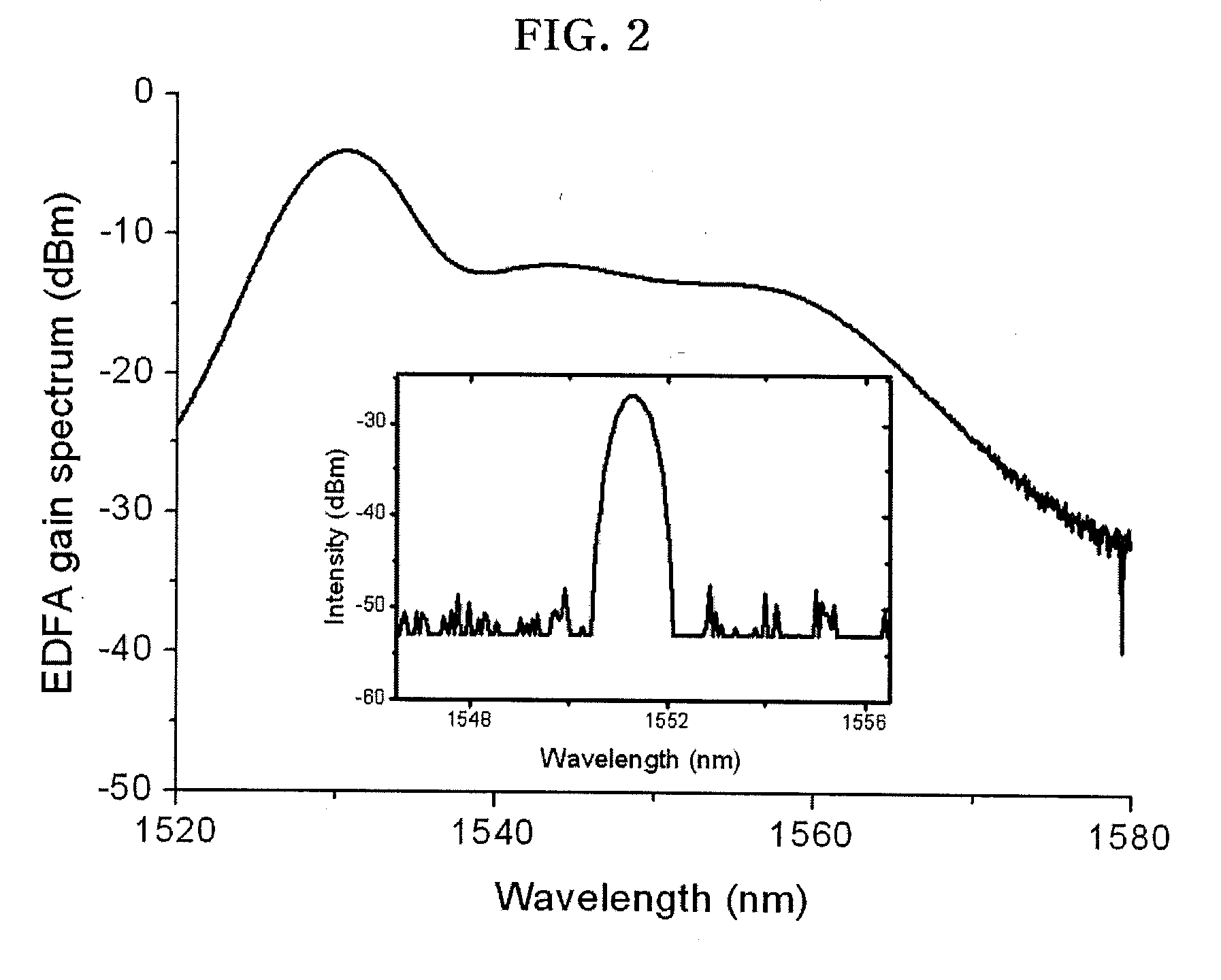
[0047]The wavelength-tunable laser system of the exemplary embodiment of the present invention of FIG. 1 was demonstrated through actual experiments. In the experiments, the EDFA was a C-band amplifier having a gain spectrum shown in FIG. 2, and a 256-phase-level 512×512-pixel Opto-VLSI processor of pixel size 15 μm was used. A spacing between the optical fiber collimator elements (the ports A and B) was 3 mm, and the optical spectrum analyzer with 0.01 nm resolution was used to monitor the laser output power generated at the 5% output port of the optical coupler (FIG. 1).
[0048]The ASE signal was collimated at 0.5 mm diameter, and a reflective grating plate, having 1200 lines / mm and a reflection angle of 70° at 1530 nm, was used to demultiplex the ASE signal and map onto an active window of the Opto-VLSI processor through a lens with a focal length of 10 cm placed 10 cm from the grating plate. The LabVIEW software was developed to generate the optimized digital holograms that steer ...
second exemplary embodiment
[0057]FIG. 4 is a schematic configuration diagram showing a wavelength-tunable laser system according to a second exemplary embodiment of the present invention. In the second exemplary embodiment, components different from those of the first exemplary embodiment will be mainly described. The description of the same components should be substituted with that of the first exemplary embodiment.
[0058]Referring to FIG. 4, the wavelength-tunable laser system includes an optical spectrum analyzer 210, optical amplifiers 220-1, . . . , 220-n, optical couplers 180-1, . . . , 180-n, an optical fiber collimator array 240, a diffraction grating plate 250, and an Opto-VLSI processor 260.
[0059]According to this exemplary embodiment, optical circulators 230-1, . . . , 230-n are disposed in correspondence with ports 240-1, . . . , 240-n of the optical fiber collimator array 240, and the optical circulators 230-1, . . . , 230-n are respectively connected to the optical amplifiers 220-1, . . . , 220-...
PUM
 Abstract
Description
Claims
Application Information


