Organic electroluminescence device

a technology of electroluminescence device and organic material, which is applied in the direction of discharge tube/lamp details, luminescnet screen of discharge tube, natural mineral layered products, etc., can solve the problems of shortening the life of the device, requiring further improvement of conventional devices, and low external quantum efficiency of devices using condensed-ring-type phosphorescent materials, etc., to achieve excellent luminous efficiency and small dependence of luminous efficiency

Active Publication Date: 2012-05-24
UDC IRELAND
View PDF4 Cites 14 Cited by
  • Summary
  • Abstract
  • Description
  • Claims
  • Application Information

AI Technical Summary

Benefits of technology

[0051]The invention can provide an organic electroluminescence device having an excellent luminous efficiency and having a small dependence of the luminous efficiency on the thickness of an electron transporting layer.

Problems solved by technology

However, such devices using the condensed-ring type phosphorescent material has a low external quantum efficiency.
According to it, however, introduction of materials which can produce an unstable oxidized species having carbazolyl groups is not preferred because it leads to shortening of the lifespan of the device.
In addition, the conventional devices are required further improvement because they do not have a sufficient luminous efficiency and moreover, the luminous efficiency may depend on the thickness of their electron transporting layer.
As described in JP-A-2009-99783, it is known that the use of materials which can produce an unstable oxidized species having carbazolyl groups is unfavorable to durability of devices.
In addition, conventional devices do not have a sufficient luminous efficiency and moreover, the luminous efficiency may depend on the thickness of the electron transporting layer so that they are required for further improvement.

Method used


Image

  • Organic electroluminescence device
  • Organic electroluminescence device
  • Organic electroluminescence device

Examples


example 1

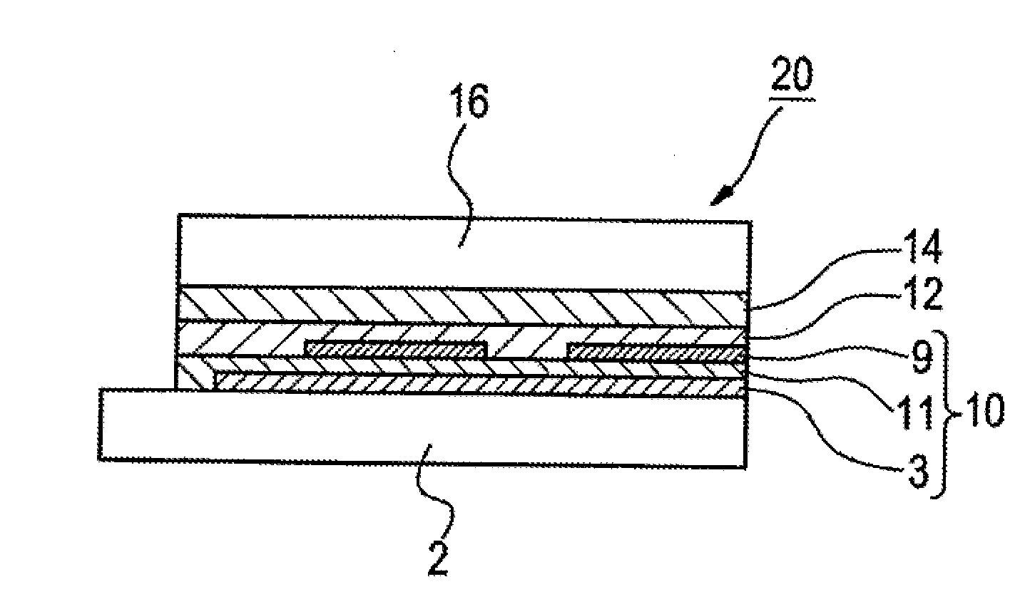
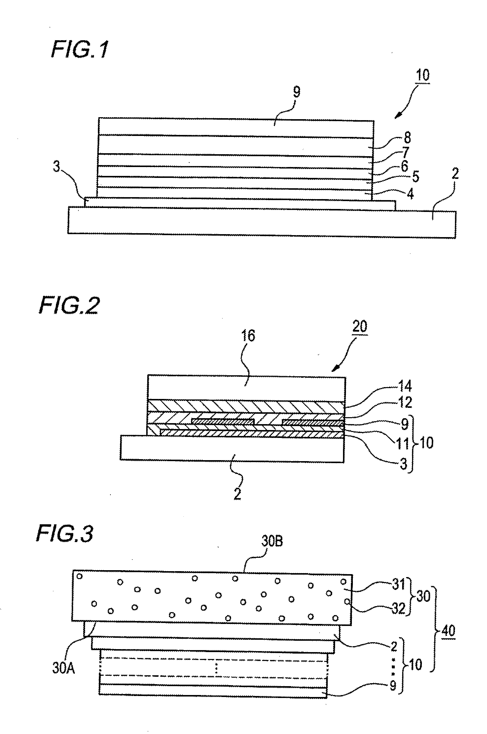
[0285]A 0.5-mm thick and 2.5-cm square glass substrate (product of Geomatec Corp., surface resistance: 10 nip) having an indium tin oxide (ITO) film was placed in a washing container. After ultrasonic washing in 2-propanol, the substrate was subjected to UV-ozone treatment for 30 minutes. The following organic layers were deposited successively on the resulting transparent anode (ITO film) by vapor deposition.

First layer: ITO / CuPc (copper phthalocyanine), film thickness: 10 nm

Second layer: NPD (N,N′-di-α-naphthyl-N,N′-diphenyl)-benzidine), film thickness: 30 nm

Third layer: dopant (10 mass %), host material (mCBP) (90 mass %), film thickness: 30 nm

Fourth layer: first electron transporting material (BAlq), film thickness: 40 nm

Fifth layer: second electron transporting material (Alq (tris(8-hydroxyquinoline)aluminum complex)), film thickness: 0 nm

[0286]Then, lithium fluoride and metal aluminum were deposited on the fifth layer to give their thicknesses of 0.2 nm and 70 nm, respectively...


PUM

PropertyMeasurementUnit
triplet excited state T1 energyaaaaaaaaaa
emission wavelengthaaaaaaaaaa
dihedral angleaaaaaaaaaa

Abstract

The organic electroluminescence device has, on a substrate thereof, a pair of electrodes and at least one organic layer including a light emitting layer between the electrodes, wherein the light emitting layer contains a phosphorescent complex material containing a specific monoanionic bidentate ligand and the device contains, in a layer sandwiched between the light emitting layer and a cathode, a compound represented by the following formula (1):
(Cz)p-L-(A)q  (1)
wherein, Cz represents a substituted or unsubstituted arylcarbazolyl or carbazolylaryl, L represents a single bond or a substituted or unsubstituted arylene, cycloalkylene, or aromatic heterocycle, A represents a substituted or unsubstituted nitrogen-containing 6-membered aromatic heterocycle, and each of p and q independently represents an integer from 1 to 6.

Description

TECHNICAL FIELD[0001]The present invention relates to an organic electroluminescence device (hereinafter, referred to also as “a device” or “an organic EL device”), and more specifically, an organic electroluminescence device which is excellent in durability at high luminance intensity.BACKGROUND ART[0002]Research and development of organic electroluminescence devices has been actively conducted in recent years because highly luminescent emission is obtained from these devices with low-voltage driving. In general, organic electroluminescence devices are constituted of an organic layer including a light-emitting layer, and a pair of electrodes between which the organic layer is sandwiched, and electrons injected from the cathode are recombined with holes injected from the anode in the light-emitting layer, to produce excitons, whose energy is utilized to luminescence.[0003]Improvement in the efficiency of devices has recently made by using a phosphorescent materials. For instance, an...

Claims


Application Information

Patent Timeline
Patent Type & Authority Applications(United States)
IPC IPC(8): H05B33/14B32B9/00
CPCC09K11/06C09K2211/1007C09K2211/1011C09K2211/1029H05B33/14H01L51/0072H01L51/0081H01L51/0085H01L51/5016C09K2211/1044H10K85/6572H10K85/324H10K85/342H10K50/11H10K2101/10
Inventor ISE, TOSHIHIROKITAMURA, TETSUTAKADA, SAKIWATANABE, TORU
Owner UDC IRELAND
Why Eureka
Try Eureka