Metal adhesion

a technology of metal adhesion and surface roughness, which is applied in the direction of semiconductor/solid-state device manufacturing, electrical apparatus, semiconductor devices, etc., can solve the problems of photovoltaic devices, poor adhesion to silicon materials, and exacerbated problems, so as to increase surface roughness and increase turbulence

Inactive Publication Date: 2012-05-31
NEWSOUTH INNOVATIONS PTY LTD
View PDF9 Cites 6 Cited by
  • Summary
  • Abstract
  • Description
  • Claims
  • Application Information

AI Technical Summary

Benefits of technology

[0006]The solar cell may include at least one hole having an undercut region resulting in an overhang under which the metallisation extends. The hole may be substantially perpendicular to the surface of the semiconductor material and the undercut region forms a ledge around a part of a periphery of an opening of the hole at the surface of the semiconductor material. The hole may also extend at an angle to the perpendicular with respect to the surface of the semiconductor material such that the hole undercuts the surface. Adjacent holes or alternate holes may extend in different directions relative to the perpendicular to further enhance the locking function.
[0011]d) plating contact metallisation over the heavily doped regions to make contact thereto, the plating extending into the intermittent surface keying features to assist in attachment of the metallisation to the semiconductor material.
[0015]In yet another method, higher energy levels are used while laser doping to create increased turbulence within the molten silicon being doped to increase the surface roughness when frozen (but without necessarily ablating silicon).
[0016]In particular the above keying methods may be used at the ends of each laser doped line where each metal finger terminates to thereby increase adhesion at these points where the metal is most likely to detach from the laser doped silicon. However these keying methods will preferably be used periodically along each laser doped line in addition to at the ends so as to provide isolated locations of good metal adhesion without significantly increasing the overall metal / silicon interface area.

Problems solved by technology

A common criticism of plated metal contacts for photovoltaic devices is the poor adhesion to the silicon material.
This problem is exacerbated when thermal cycling occurs due to the thermal expansion mismatch between the silicon and the metal and also when low metal / silicon interface area is used which is common in high performance cells due to the improved electrical performance.
There is consequently often a trade-off between electrical performance and durability.
Subsequent metal adhesion to such surfaces, as shown in FIG. 10, is therefore a challenge.

Method used


Image

  • Metal adhesion
  • Metal adhesion
  • Metal adhesion

Examples


Embodiment Construction

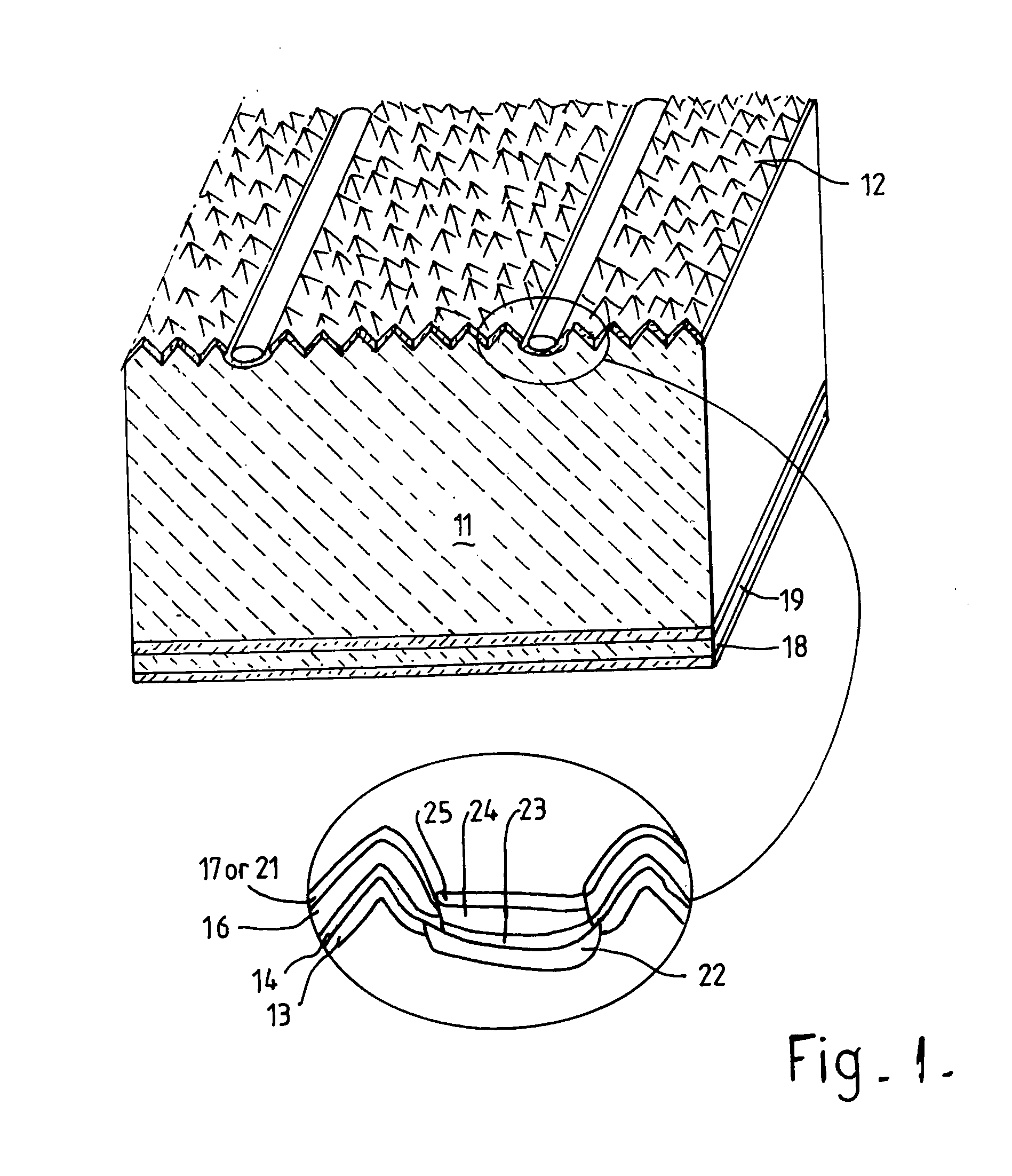
[0030]By way of example, and with reference to FIG. 1, a suitable fabrication sequence for the formation of a silicon solar cell is as follows:

1. Isotropic texturing 12 of the front (or light receiving) surface of the p-type wafer 11;

2. front surface diffusion of n-type dopant 13;

3. edge junction isolation / psg removal;

4. ARC deposition on the front surface by PECVD;[0031]a. 100 angstroms of hydrogen rich silicon nitride specifically for surface passivation 14;[0032]c. 600 angstroms of silicon nitride 16 of refractive index 2.0-2.1;[0033]d. dopant containing layer 17;

5. screen-print rear (non-light receiving) surface with aluminium for rear contact 18;

6. fire rear surface to sinter rear contacts 18 and form back surface field 19 by formation of aluminium / silicon alloy and liquid phase epitaxy;

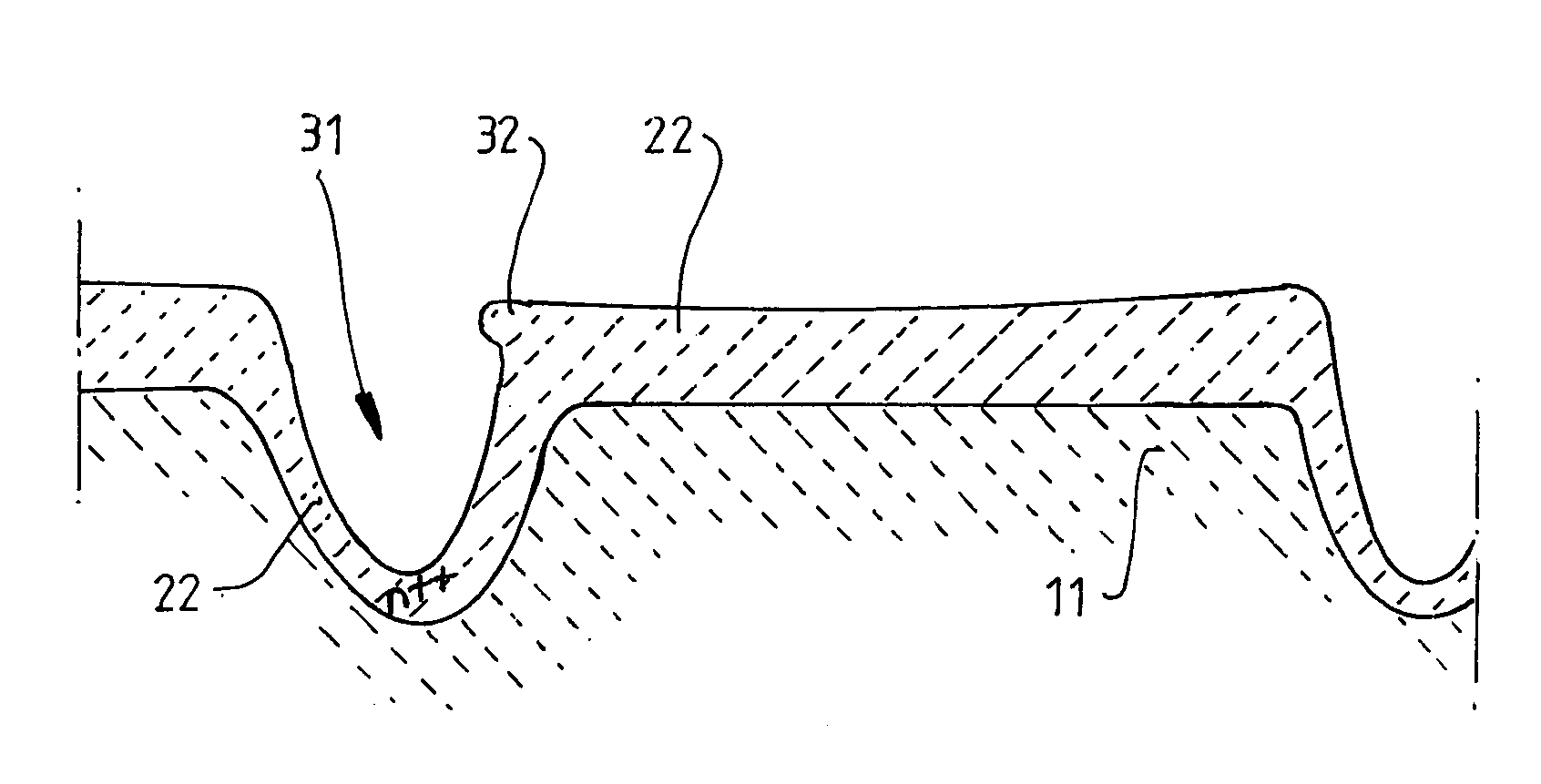
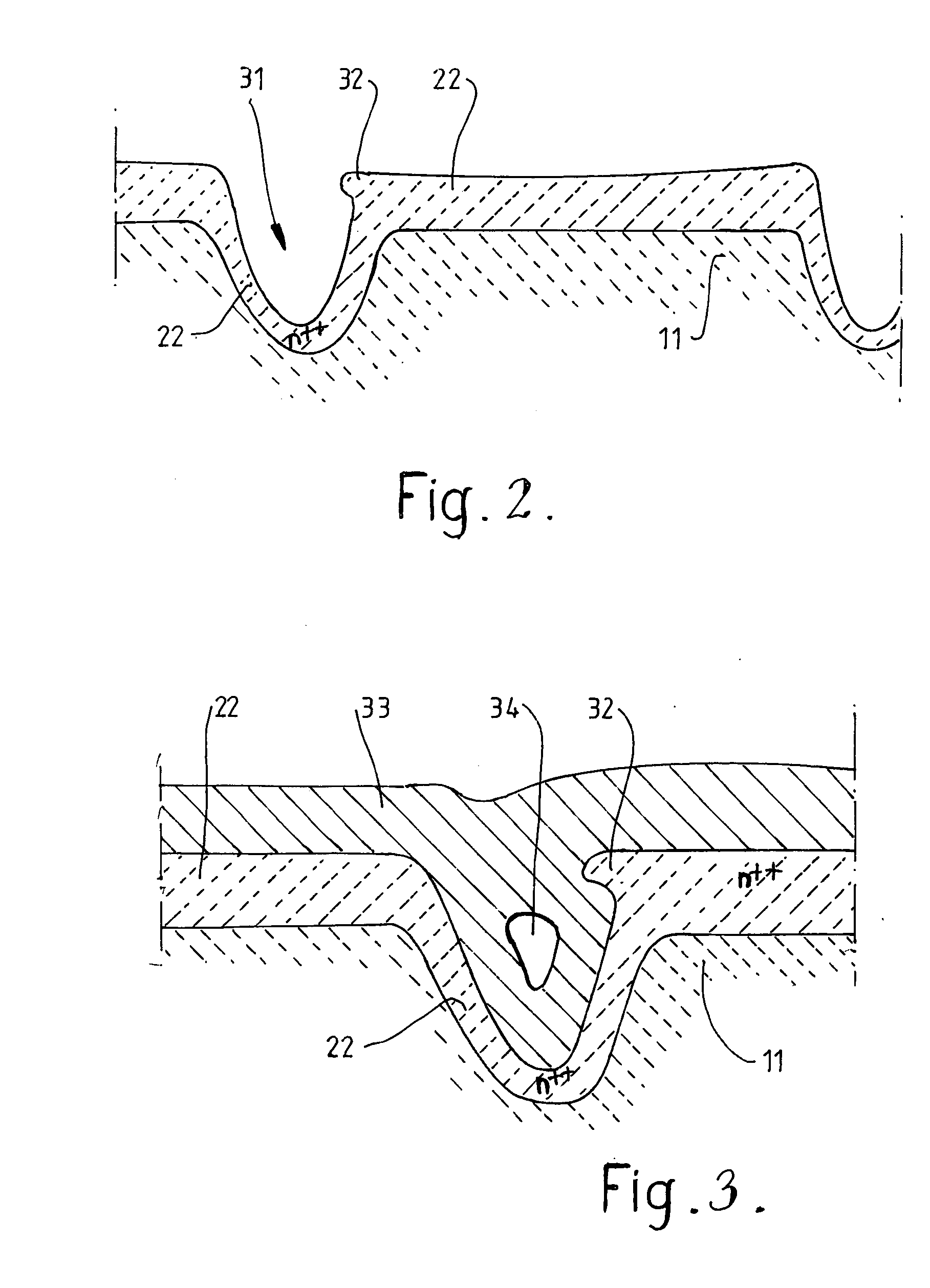
7. laser doping of silicon in localised regions to form heavily doped (n+) regions 22 for formation of self-aligned front surface metal contacts;

8. Plating a layer of Nickel 23 over the laser do...


PUM

PropertyMeasurementUnit
depthsaaaaaaaaaa
depthsaaaaaaaaaa
angleaaaaaaaaaa

Abstract

A solar cell has a metal contact formed to electrically contact a surface of semiconductor material forming a photo-voltaic junction. The solar cell includes a surface region or regions of heavily doped material and the contact comprises a contact metallisation formed over the heavily doped regions to make contact thereto. Surface keying features are located in the semiconductor material into which the metallisation extends to assist in attachment of the metallisation to the semiconductor material.

Description

INTRODUCTION[0001]The present invention relates generally to the field of photovoltaics and in particular an improved method of creating contacts is disclosed.BACKGROUND[0002]A common criticism of plated metal contacts for photovoltaic devices is the poor adhesion to the silicon material. This problem is exacerbated when thermal cycling occurs due to the thermal expansion mismatch between the silicon and the metal and also when low metal / silicon interface area is used which is common in high performance cells due to the improved electrical performance. There is consequently often a trade-off between electrical performance and durability. The laser doped solar cell faces the same challenges [S. R. Wenham, M. A. Green “A Self-Aligning Method for Forming a Selective Emitter and Metallization in a Solar Cell”, International Patent No. PCT / AU / 1999 / 00522, July, 1999], with the best electrical performance achieved when the laser doped region is flat and smooth which also corresponds to the...

Claims


Application Information

Patent Timeline
Patent Type & Authority Applications(United States)
IPC IPC(8): H01L31/0224H01L31/0236
CPCH01L21/268Y02E10/50H01L31/022425
Inventor WENHAM, ALISON MAREEGREEN, MARTIN ANDREWWENHAM, STUART ROSS
Owner NEWSOUTH INNOVATIONS PTY LTD
Why Eureka
Try Eureka