Semiconductor structures having improved contact resistance

a technology of semiconductors and structures, applied in the field of semiconductor structures, can solve problems such as reducing the contact resistance of structures

Active Publication Date: 2012-05-31
GLOBALFOUNDRIES US INC
View PDF27 Cites 37 Cited by
  • Summary
  • Abstract
  • Description
  • Claims
  • Application Information

AI Technical Summary

Benefits of technology

[0029]providing at least one field effect transistor upon and within a surface of a semiconductor substrate, said at least one field effect transistor including source and drain diffusion regio

Problems solved by technology

The presence of the ordered, nanosized pattern within a material present in the conductive contact region increases the o

Method used


Image

  • Semiconductor structures having improved contact resistance
  • Semiconductor structures having improved contact resistance
  • Semiconductor structures having improved contact resistance

Examples


first embodiment

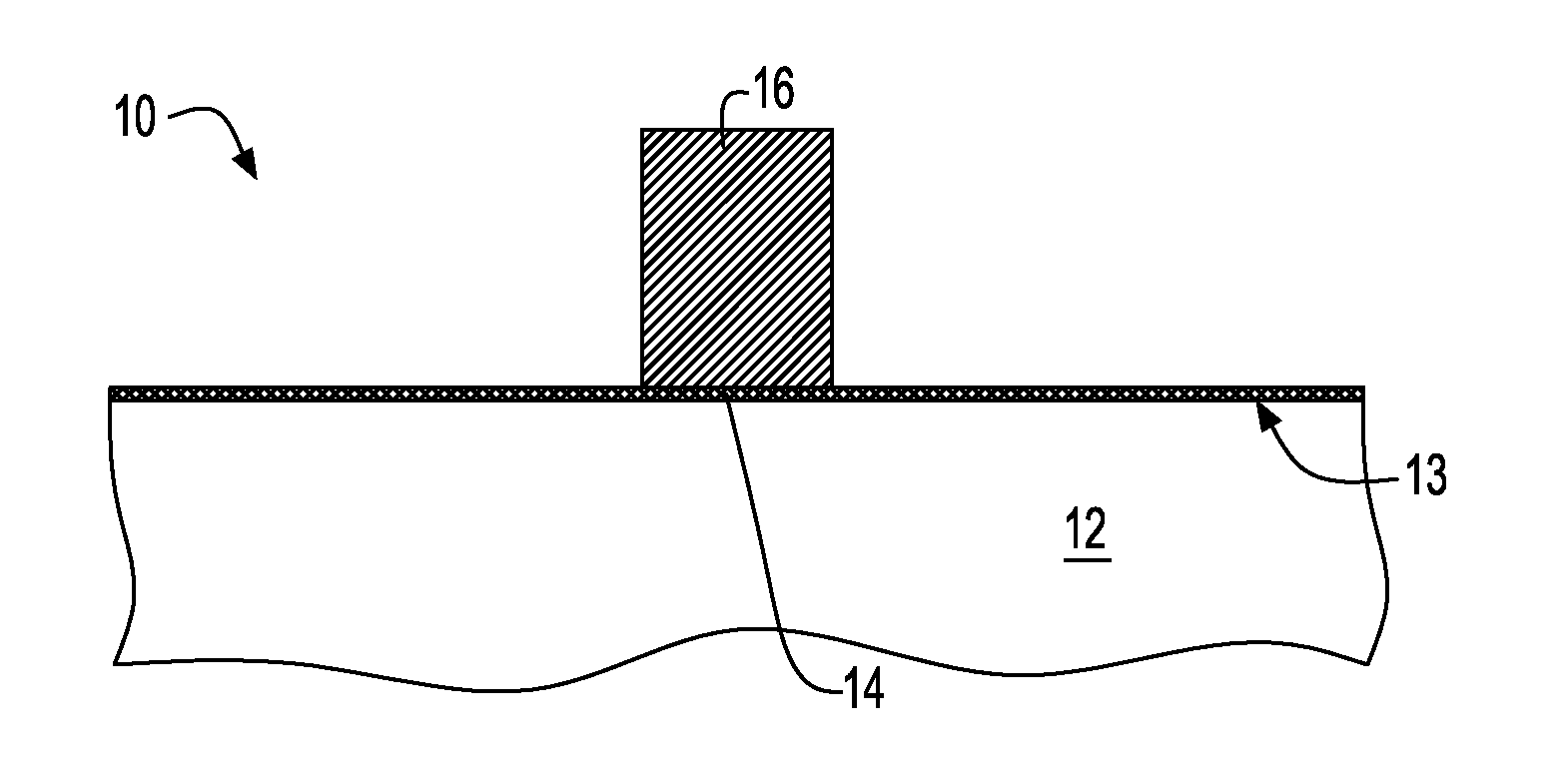
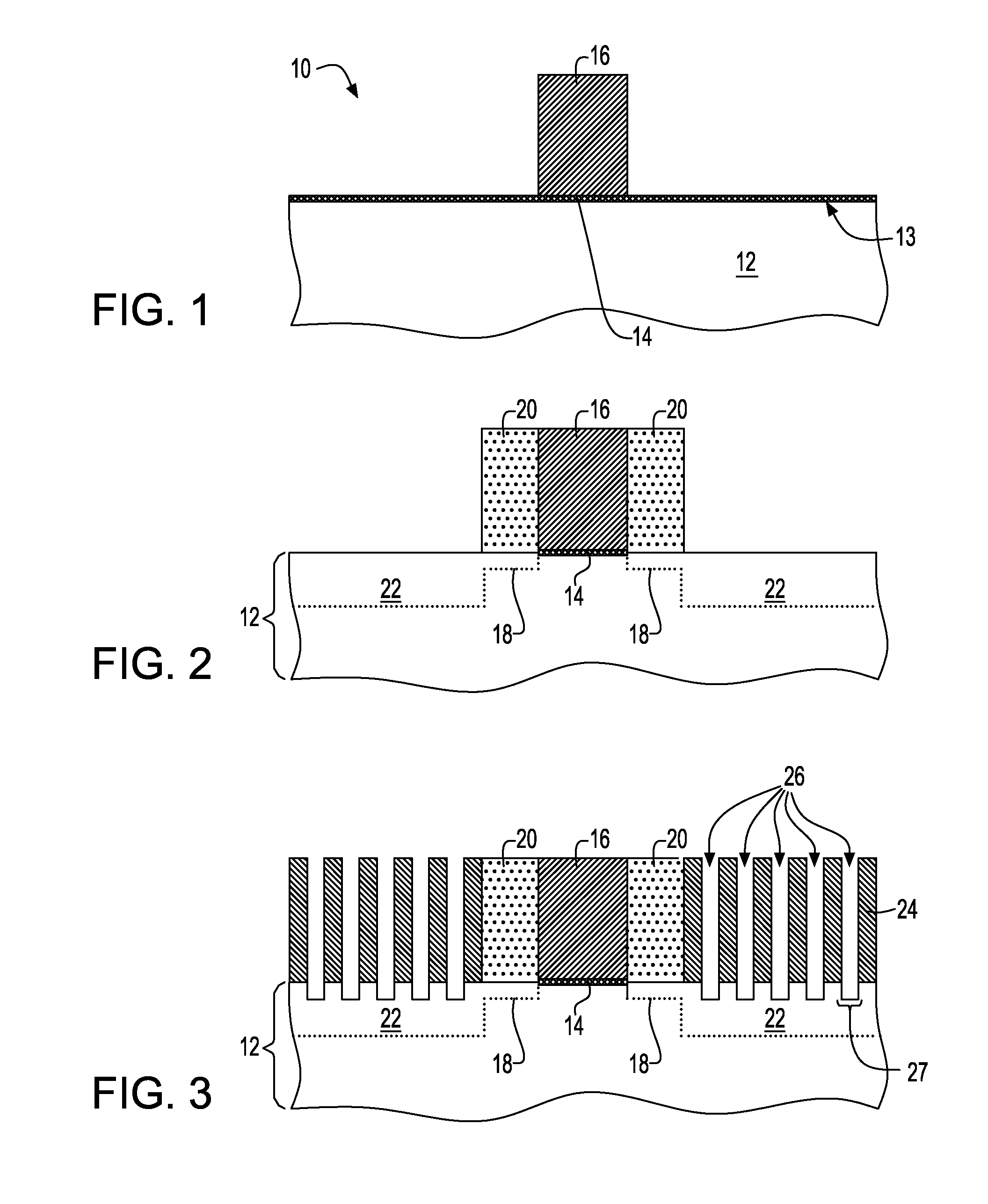
[0047]FIG. 1 illustrates an initial structure 10 that is formed in this first embodiment of the present invention. The initial structure 10 includes a semiconductor substrate 12 having an upper surface 13. Atop the upper surface 13 there is a gate dielectric 14 and a patterned gate conductor 16. The initial structure shown in FIG. 1 can be formed utilizing conventional techniques well known to those skilled in the art. For example, deposition, lithography and etching can be used. Alternatively, a replacement gate process can be used to provide the initial structure 10 shown in FIG. 1. Since both of these techniques are well known to those skilled in the art, processing details have been omitted so as not to obscure the invention.

[0048]The semiconductor substrate 12 employed in the initial structure 10 comprises any semiconducting material including, but not limited to: Si, Ge, SiGe, SiC, SiGeC, Ge, GaAs, GaN, InAs, InP and all other III / V or II / VI compound semiconductors. Semiconduc...

second embodiment

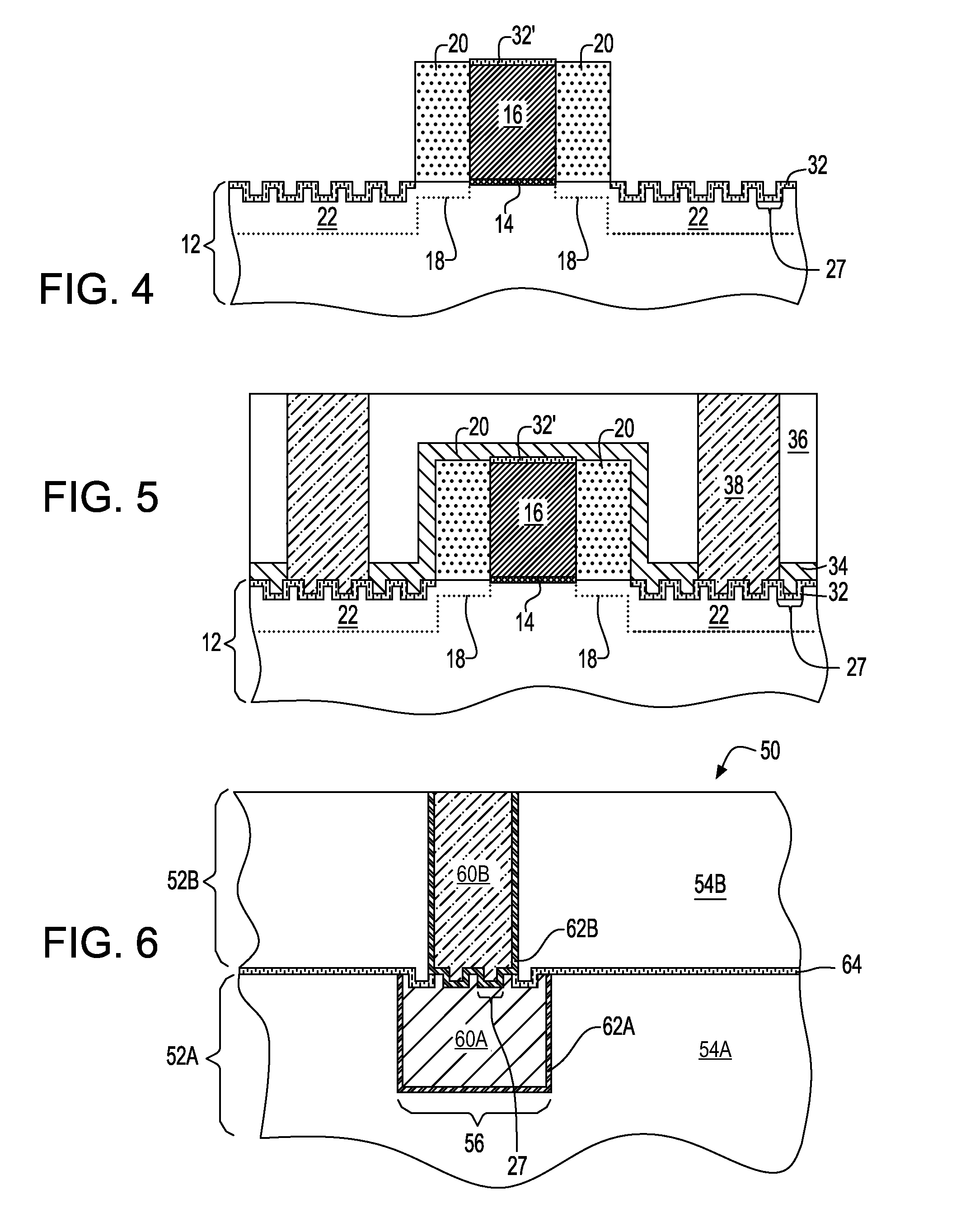
[0095]Reference is now made to FIG. 6 which illustrates the present invention. In the second of the present invention, self-assembled polymer technology is used in improving the contact resistance of an interconnect structure 50. That is, the contact resistance is improved in a contact region between a first conductive material and a second conductive material.

[0096]The interconnect structure 50 includes a lower interconnect level 52A that comprises a first interconnect dielectric material 54A which includes at least one wiring region 56 located therein. The at least one wiring region 56 includes an opening that is filled with a conductive material 60A and is lined with a diffusion barrier 62A. The first interconnect dielectric material 54A includes one of the dielectric materials described above for dielectric material 36 in the first embodiment. The diffusion barrier includes one of Ti, Ta, W TaN, TiN and WN, and the conductive material includes, for example, doped polySi, W, Al, ...


PUM


Abstract

Self-assembled polymer technology is used to form at least one ordered nanosized pattern within material that is present in a conductive contact region of a semiconductor structure. The material having the ordered, nanosized pattern is a conductive material of an interconnect structure or semiconductor source and drain diffusion regions of a field effect transistor. The presence of the ordered, nanosized pattern material within the contact region increases the overall area (i.e., interface area) for subsequent contact formation which, in turn, reduces the contact resistance of the structure. The reduction in contact resistance in turn improves the flow of current through the structure. In addition to the above, the inventive methods and structures do not affect the junction capacitance of the structure since the junction area remains unchanged.

Description

FIELD OF THE INVENTION [0001]The present invention relates to semiconductor structures and methods of fabricating the same. More particularly, the present invention relates to semiconductor structures such as, for example, field effect transistors (FETs) and interconnect structures, having improved contact resistance.BACKGROUND OF THE INVENTION[0002]An important property of high performance semiconductor devices is the ability to conduct electricity. Current is inversely related to resistance. Traditionally, increasing the cross-section of the semiconducting material, shortening the length for the electron path, increasing the voltage, or decreasing the resistivity of the semiconducting material can all decrease resistance and increase electron flow through electrical devices.[0003]In order to be able to make integrated circuits (ICs), such as memory, logic, and other devices, of higher integration density than currently feasible, one has to find ways to further downscale the dimens...

Claims


Application Information

Patent Timeline
IPC IPC(8): H01L29/78H01L21/768H01L23/52
CPCB81B2207/07B81C1/00095B81C2201/0149H01L21/28518H01L21/3086H01L21/76886H01L23/485H01L2924/0002H01L23/5226H01L29/41766H01L29/665H01L29/66636H01L2924/00
Inventor DORIS, BRUCE B.RADENS, CARL J.STAMPER, ANTHONY K.STRANE, JAY W.
Owner GLOBALFOUNDRIES US INC
Why Eureka
Try Eureka