Semiconductor film, method for manufacturing the same, and power storage device

a technology of semiconductor film and semiconductor film, which is applied in the direction of semiconductor/solid-state device details, cell components, electrochemical generators, etc., can solve the problems of difficult to achieve high-density formation, and achieve the effect of improving charge-discharge capacity and enhancing chemical vapor deposition

Active Publication Date: 2012-05-31
SEMICON ENERGY LAB CO LTD
View PDF0 Cites 8 Cited by
  • Summary
  • Abstract
  • Description
  • Claims
  • Application Information

AI Technical Summary

Benefits of technology

[0012]The present invention is made in view of the foregoing technical background. Accordingly, an object of one embodiment of the present invention is to provide a semiconductor film including silicon microstructures formed at high density and a manufacturing method thereof Further, an object of one embodiment of the present invention is to provide a semiconductor film including silicon microstructures whose density is controlled, and a manufacturing method thereof Furthermore, an object of one embodiment of the present invention is to provide a power storage device with improved charge-discharge capacity.
[0013]In order to achieve the above objects, the present invention focuses on silicon microstructures formed over a metal surface. The silicon microstructures are formed in such a manner that a silicon film is formed over a metal surface by a deposition method such as a low pressure chemical vapor deposition (LPCVD) method or a plasma enhanced chemical vapor deposition (PECVD) method.
[0014]As a result of earnest study of formation mechanism of the silicon structures, the present inventors have found that projections and depressions are formed in the vicinity of a surface of a silicide layer due to compressive stress generated due to volume expansion in silicide reaction of a metal, and that a grain size of a silicide grain which is detached from the projection is closely related to the shape of the silicon structure.
[0015]Further, the present inventors have arrived at the invention of a semiconductor film including silicon structures of various shapes, which are formed by controlling the grain sizes of silicide grains which are nuclei of growth of the silicon structures.
[0016]For example, in the case where a needle-like silicon whisker is formed, a minute silicide grain may be generated only in the vicinity of a surface by silicide reaction and a silicon structure may be formed using the silicide grain as a nucleus of growth. When silicide reaction is caused only in the vicinity of a surface, compressive stress generated due to volume expansion accompanying the silicide reaction concentrates in a direction toward the surface of the silicide layer; thus, in the surface of the silicide layer, the height difference of the depressions and the projections becomes large and the interval of the same becomes small. As a result, the silicide grain which is detached from the projection of the surface of the silicide layer becomes extremely minute, and a silicon structure which grows from the minute silicide grain is likely to become a needle-like silicon whisker. A semiconductor film including a needle-like silicon whisker formed by such a method includes a minute silicide grain in the vicinity of an interface between a silicon layer and the silicide layer. The grain size of the silicide grain is greater than or equal to 1 nm and less than 50 nm.
[0017]In contrast, in the case where a large silicide grain is formed, silicide reaction preferably proceeds deep in a film thickness direction (toward a metal layer). In that case, compressive stress generated due to volume expansion accompanying the silicide reaction is relieved in the film thickness direction. As a result, the height difference of the depressions and the projections becomes small and the interval of the same becomes large. Accordingly, the grain size of the silicide grain detached from the projection becomes large. A silicon structure which grows from the thus obtained large silicide grain is likely to have not a needle-like shape but a hemispherical (dome-like) shape. A semiconductor film including a hemispherical (dome-like) silicon structure manufactured by such a method includes a large silicide grain around an interface between a silicon layer and the silicide layer. The grain size of the silicide grain is greater than or equal to 50 nm.

Problems solved by technology

However, it has been difficult to achieve high-density formation by a method for manufacturing a silicon nanoneedle using a conventional VLS growth method.

Method used


Image

  • Semiconductor film, method for manufacturing the same, and power storage device
  • Semiconductor film, method for manufacturing the same, and power storage device
  • Semiconductor film, method for manufacturing the same, and power storage device

Examples


embodiment 1

[0050]In this embodiment, according to one embodiment of the present invention, a semiconductor film including a silicon structure and a manufacturing method thereof will be described with reference to FIGS. 1A and 1B, FIGS. 2A and 2B, FIGS. 3A and 3B, and FIG. 4.

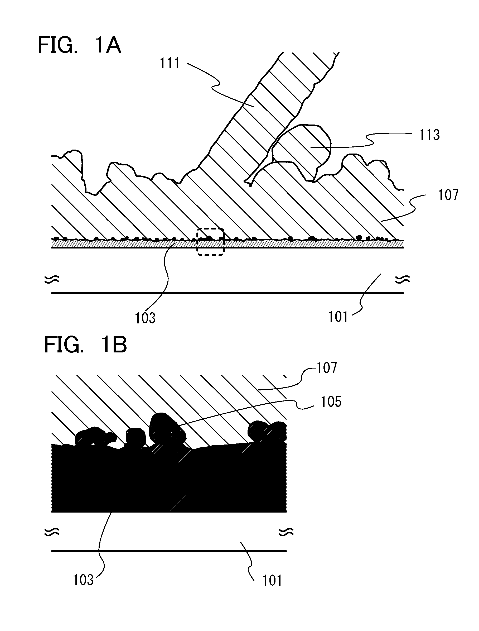
[0051]FIG. 1A is a schematic cross-sectional view of a semiconductor film including needle-like silicon whiskers, which is described in this embodiment.

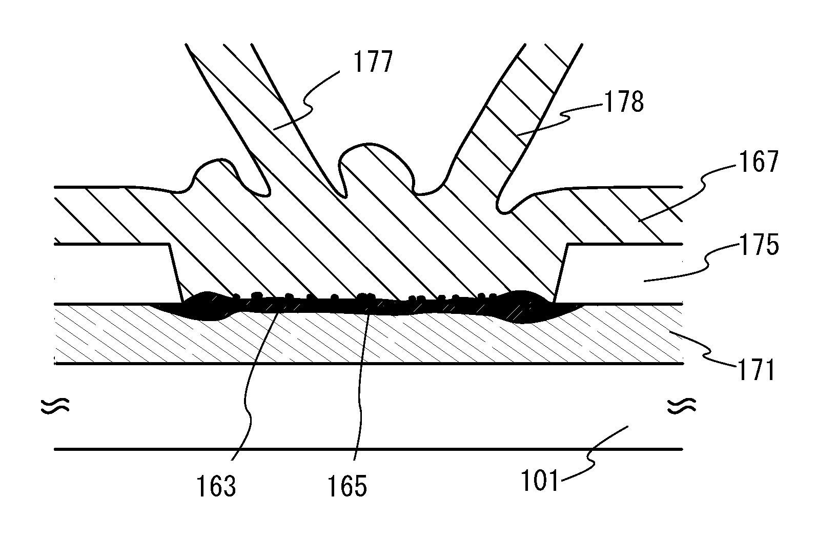
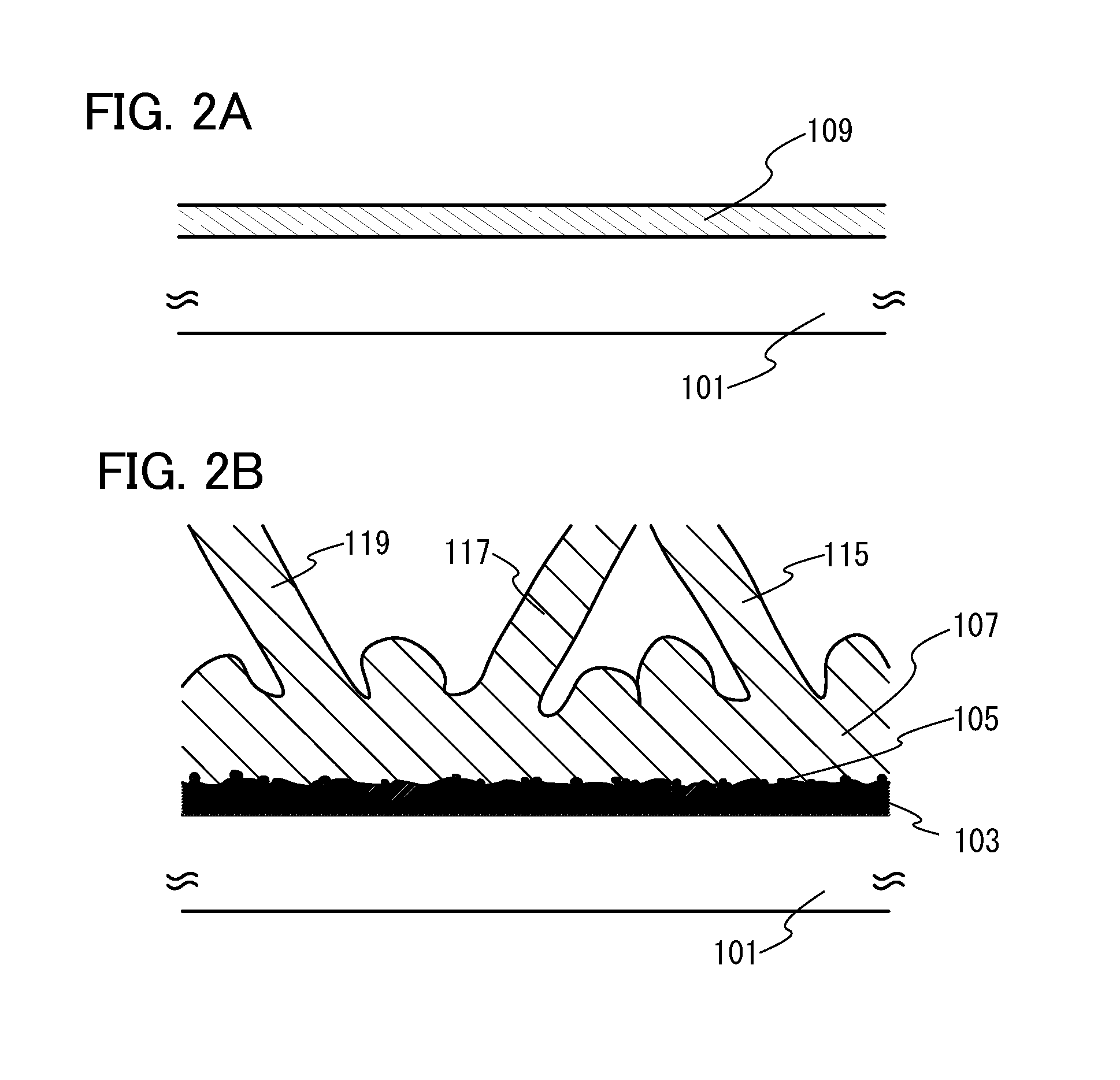
[0052]The semiconductor film according to one embodiment of the present invention is formed over a substrate 101 and includes a silicide layer 103, minute silicide grains 105 over the silicide layer 103, and a silicon layer 107 which is in contact with the silicide layer 103 and the silicide grains 105 and covers the silicide layer 103 and the silicide grains 105. The silicon layer 107 includes needle-like silicon whiskers 111 and 113.

[0053]The silicide layer 103 includes a silicide resulting from reaction of a metal included in a metal layer 109 described later and silicon....

modification example 1

[0081]Next, a semiconductor film which includes needle-like silicon whiskers and has a different structure from the above, and a manufacturing method thereof will be described with reference to FIGS. 3A and 3B.

[0082]A semiconductor film illustrated in FIG. 3B, which includes needle-like silicon whiskers, includes a silicide layer 123 which is formed by making the vicinity of a substrate 121 including a metal into silicide, and also includes a large number of silicide grains 125 in the vicinity of or adjacent to a surface of the silicide layer 123. Further, a silicon layer 127 including a plurality of needle-like silicon whiskers (silicon whiskers 131, 133, and 135) is included so as to be in contact with and to cover the silicide layer 123 and the large number of silicide grains 125.

[0083]The structure of the semiconductor film illustrated in FIG. 3B, which includes the needle-like silicon whiskers, is different from the above structure in that the silicide layer 123 is formed in su...

modification example 2

[0089]In contrast to the above-described method for manufacturing needle-like silicon whiskers, a silicon microstructure having a shape different from the needle-like silicon whiskers can be manufactured in such a manner that the thickness of a silicide layer which is formed by reaction with silicon is greater than or equal to 100 nm and the grain size of each silicide grain is greater than or equal to 50 nm.

[0090]FIG. 4 is a schematic cross-sectional view of a semiconductor film including silicon structures formed over the substrate 101, which is one embodiment of the present invention.

[0091]The semiconductor film illustrated in FIG. 4, which includes dome-like silicon structures, includes a metal layer 149 over the substrate 101, a silicide layer 143 which is formed in such a manner that the vicinity of a surface of the metal layer 149 is silicided, and a large number of silicide grains 145 in the vicinity of or adjacent to a surface of the silicide layer 143. Further, a silicon l...


PUM

PropertyMeasurementUnit
thicknessaaaaaaaaaa
thicknessaaaaaaaaaa
grain sizeaaaaaaaaaa

Abstract

Provided are a semiconductor film including silicon microstructures formed at high density, and a manufacturing method thereof. Further, provided are a semiconductor film including silicon microstructures whose density is controlled, and a manufacturing method thereof Furthermore, a power storage device with improved charge-discharge capacity is provided. A manufacturing method in which a semiconductor film with a silicon layer including silicon structures is formed over a substrate with a metal surface is used. The thickness of a silicide layer formed by reaction between the metal and the silicon is controlled, so that the grain sizes of silicide grains formed at an interface between the silicide layer and the silicon layer are controlled and the shapes of the silicon structures are controlled. Such a semiconductor film can be applied to an electrode of a power storage device.

Description

BACKGROUND OF THE INVENTION[0001]1. Field of the Invention[0002]The present invention relates to a semiconductor film and a method for manufacturing the semiconductor film. The present invention relates to a power storage device.[0003]Note that the power storage device refers to all elements and devices which have a function of storing power.[0004]2. Description of the Related Art[0005]In recent years, high-performance power storage devices such as lithium-ion secondary batteries, lithium-ion capacitors, and air cells have been developed.[0006]An electrode for the power storage device is manufactured by providing an active material over a surface of a current collector. As the active material, a material such as carbon or silicon, which can store and release ions serving as carriers, is used. For example, silicon or phosphorus-doped silicon has higher theoretical capacity than carbon and is advantageous in increasing the capacity of a power storage device (e.g., Patent Document 1).[...

Claims


Application Information

Patent Timeline
Patent Type & Authority Applications(United States)
IPC IPC(8): H01M4/13H01L21/28H01M4/02H01L29/02H01G11/06H01G11/22H01G11/30H01G11/48H01M4/134H01M4/1395
CPCH01M4/0428H01M4/134Y02E60/122H01M4/386H01L29/12H01M4/366Y02E60/10H01M10/0525
Inventor YOKOI, TOMOKAZUINOUE, TAKAYUKIFURUNO, MAKOTO
Owner SEMICON ENERGY LAB CO LTD
Why Eureka
Try Eureka