Full-spectrum absorption solar cell

a solar cell, full-spectrum technology, applied in the field of solar cells, can solve the problems of poor photoelectric conversion efficiency, increased fabrication cost, and high cost of furnace process, and achieve the effects of improving the absorption of short-spectrum, high cost, and complicated fabrication process

Inactive Publication Date: 2012-06-21
NATIONAL TSING HUA UNIVERSITY
View PDF2 Cites 7 Cited by
  • Summary
  • Abstract
  • Description
  • Claims
  • Application Information

AI Technical Summary

Benefits of technology

[0006]The primary objective of the present invention is to solve the problem that the conventional solar cell is fabricated at a higher cost.
[0007]Another objective of the present invention is to solve the problem that the conventional full-spectrum absorption solar cell is made of multilayer materials and has a complicated fabrication process.
[0008]To achieve the abovementioned objectives, the present invention proposes a full-spectrum absorption solar cell, which comprises a substrate, a first electrode layer on the substrate, a P-type semiconductor layer, an N-type cobalt-doped layer, and a second electrode layer. The P-type semiconductor layer is arranged at one side of the first electrode layer far from the substrate and connected with the first electrode layer. The N-type cobalt-doped layer is arranged at one side of the P-type semiconductor layer far from the first electrode layer and connected with the P-type semiconductor layer. The N-type cobalt-doped layer is made of a cobalt-doped tin dioxide (Sn1-XCOXO2) and connected with the P-type semiconductor layer to form a depletion layer at the junction thereof. The depletion layer absorbs light and generates electron-hole pairs. The second electrode layer is arranged at one side of the N-type cobalt-doped layer far from the first electrode layer and connected with the N-type cobalt-doped layer. Via optical characteristic analysis of oxide, it is known that the absorption spectrum of the cobalt-doped tin dioxide ranges from 700 nm to 1400 nm. The P-type semiconductor layer is made of cuprous oxide (Cu2O) havi

Problems solved by technology

However, the cost and energy loss of the furnace process are much higher, thus is increased the fabrication cost.
However, it has poor photoelectric conversion efficiency.
A common solar cell can only absorb a part of the sunlight spectrum, such that other sunlight spectrum is

Method used


Image

  • Full-spectrum absorption solar cell
  • Full-spectrum absorption solar cell
  • Full-spectrum absorption solar cell

Examples


Embodiment Construction

[0013]The technical contents of the present invention are described in detail in cooperation with the drawings below.

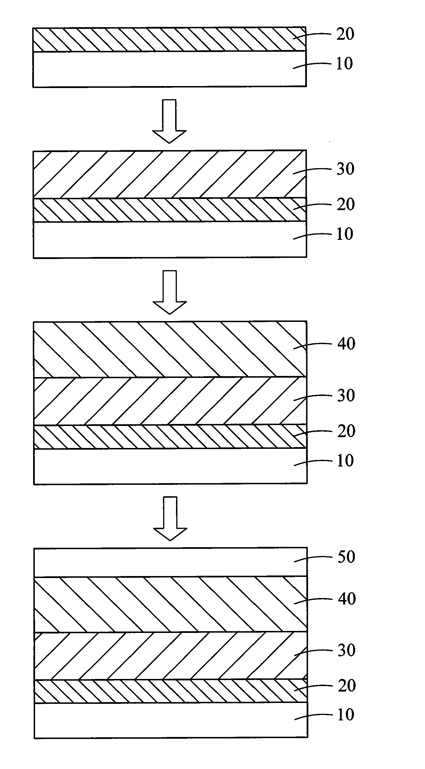
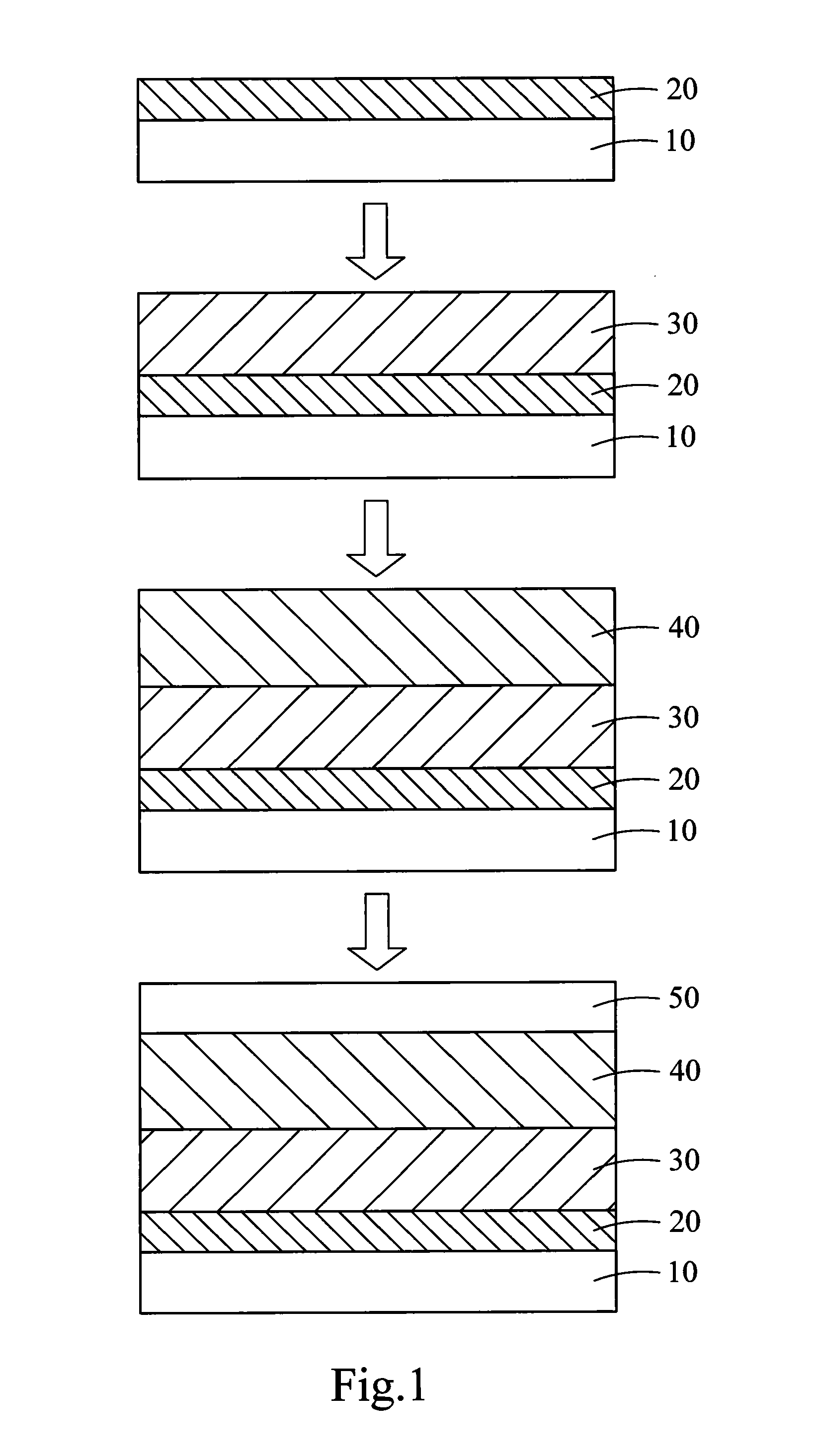
[0014]Refer to FIG. 1 a diagram schematically showing the fabrication process of a full-spectrum absorption solar cell according to one embodiment of the present invention. The full-spectrum absorption solar cell of the present invention comprises a substrate 10, a first electrode layer 20 formed on the substrate 10, a P-type semiconductor layer 30, an N-type cobalt-doped layer 40, and a second electrode layer 50. The substrate 10 is made of a material selected from a group consisting of silicon chip, glass or plastic. In this embodiment, the first electrode layer 20 is made of a material selected from a group consisting of platinum, titanium and a combination thereof. The first electrode layer 20 has the metal opaque characteristic and reflects incident light. The P-type semiconductor layer 30 is arranged at one side of the first electrode layer 20 far from the subst...


PUM


Abstract

A full-spectrum absorption solar cell adopts cobalt-doped tin dioxide as an N-type material. Thereby, a solar cell of the present invention can be fabricated by a spray method in a hot pressing fabrication process. The present invention does not need to fabricate a solar cell in a vacuum or furnace system and thus can solve the high cost problem of the conventional technology. The N-type cobalt-doped layer can absorb full spectrum of sunlight. The N-type cobalt-doped layer can be used to fabricate a solar cell with a low-temperature fabrication process. Thus, the present invention does not need to adopt a high-temperature resistant substrate (such as silicon chip or glass) used in the conventional high-temperature fabrication process but can adopt a substrate made of plastic. And, the conversion efficiency of the invention can achieve 1.2%, it is a significant improvement over the oxide-based nanostructures heterojunction solar cells in the world.

Description

FIELD OF THE INVENTION[0001]The present invention relates to a solar cell, particularly to a full-spectrum absorption solar cell.BACKGROUND OF THE INVENTION[0002]Various alternative energies have been developed to solve the problem of petroleum exhaustion. Among them, solar energy attracts the most attention because it has features of inexhaustibility and non-pollution. In a solar cell, a depletion region is formed between a P-type semiconductor material and an N-type semiconductor material to absorb solar energy and converts the solar energy into electric energy. The combinations of different materials and fabrication environments result in different photoelectric efficiency.[0003]For instance, Jingbiao Cui and Ursula J. Gibson disclosed “A Simple Two-Step Electrodeposition of Cu2O / ZnO Nanopillar Solar Cells” in the Journal of Physical Chemistry C, 2010, 114, p6804-6412, wherein a cuprous oxide film is used as the P-type semiconductor material, and a zinc oxide film is used as the ...

Claims


Application Information

Patent Timeline
IPC IPC(8): H01L31/0256
CPCH01L31/032H01L31/0321Y02E10/50H01L31/072H01L31/18H01L31/0336
Inventor SHIU, HUI-YINGYEW, TRI-RUNG
Owner NATIONAL TSING HUA UNIVERSITY
Why Eureka
Try Eureka