Semiconductor device and method for manufacturing the same

a technology of semiconductors and semiconductors, applied in the direction of semiconductor devices, basic electric elements, electrical apparatus, etc., can solve the problems of short channel effect and likely cause of threshold voltage drop, and achieve the effect of easy miniaturization, favorable electric characteristics and reliability

Active Publication Date: 2012-06-28
SEMICON ENERGY LAB CO LTD
View PDF11 Cites 81 Cited by
  • Summary
  • Abstract
  • Description
  • Claims
  • Application Information

AI Technical Summary

Benefits of technology

[0027]According to one embodiment of the present invention, a semiconductor device which includes an oxide sem

Problems solved by technology

This phenomenon is called a short-channel effect, and suppression of the short-channel effect is a challenge for miniaturization of a transistor.
In additio

Method used


Image

  • Semiconductor device and method for manufacturing the same
  • Semiconductor device and method for manufacturing the same
  • Semiconductor device and method for manufacturing the same

Examples


embodiment 1

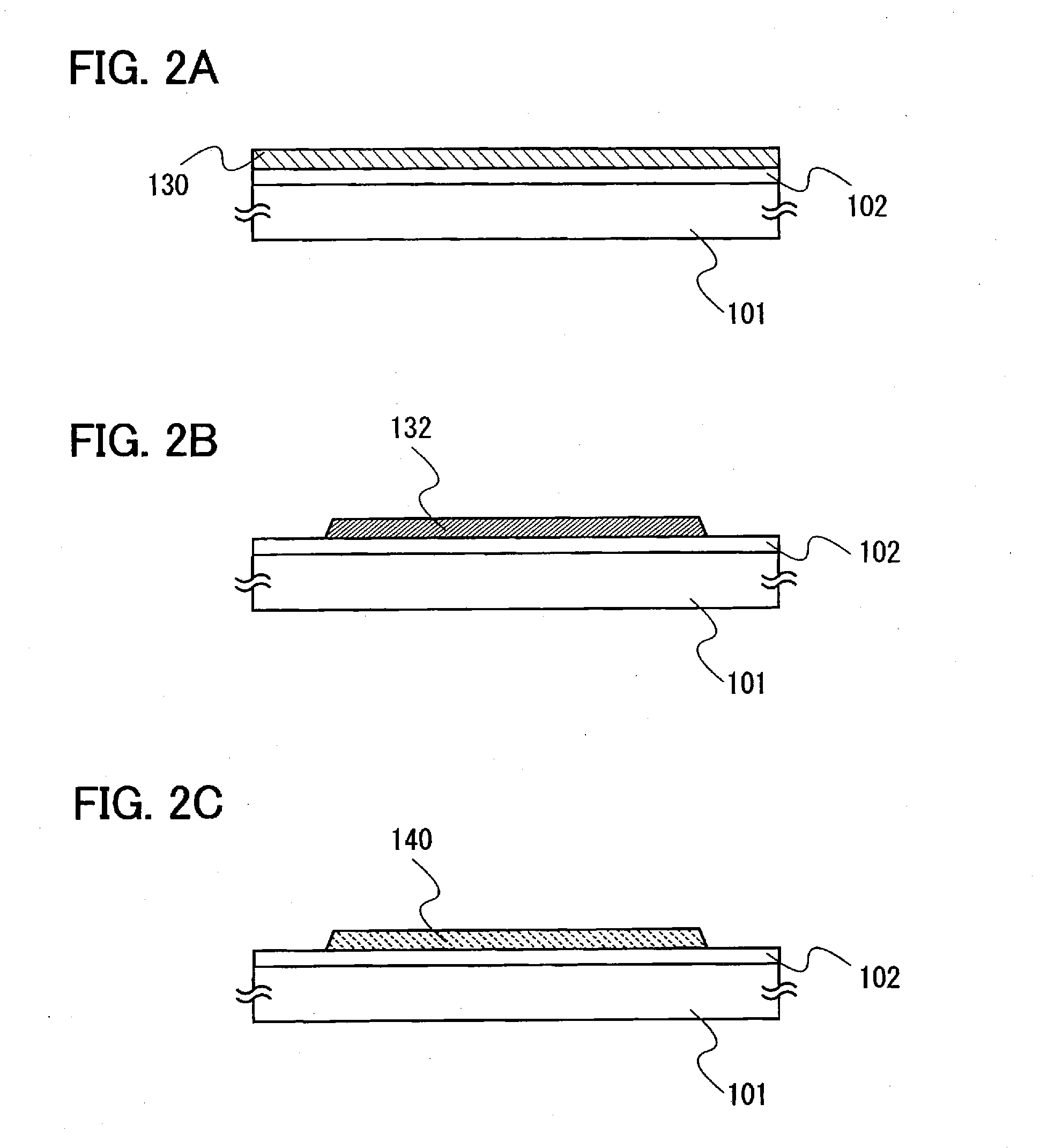
[0048]In this embodiment, a structure of a transistor which is one embodiment of the present invention and a method for manufacturing the transistor will be described with reference to FIGS. 1A and 1B, FIGS. 2A to 2C, and FIGS. 3A to 3E.

(Structure and Characteristic of Transistor 100)

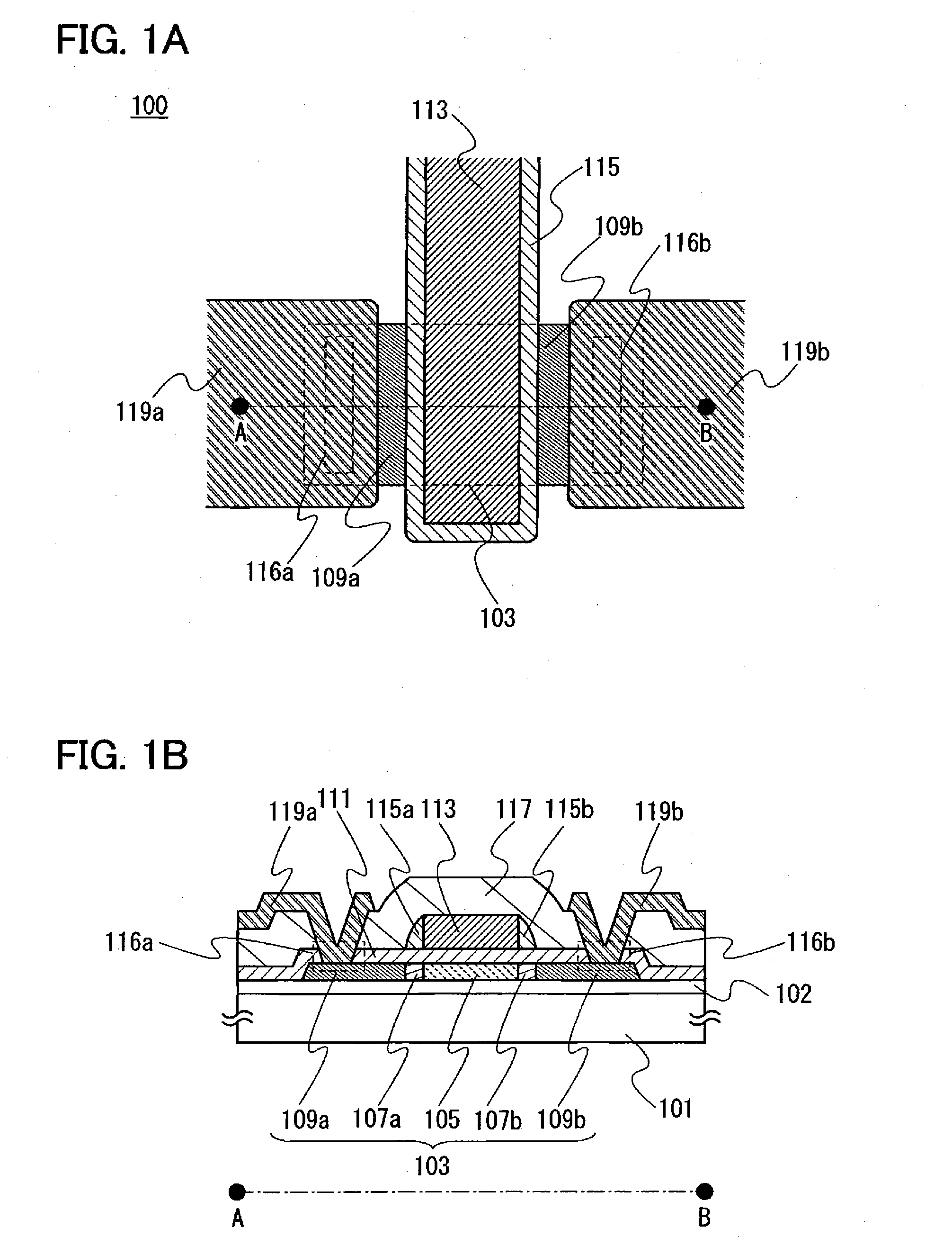
[0049]FIG. 1A is a plan view of a transistor 100. Note that a base insulating film 102, a gate insulating film 111, and an interlayer insulating film 117 are not illustrated in FIG. 1A for convenience.

[0050]In FIG. 1A, a first electrode 113 and a sidewall insulating film 115 on side surfaces of the first electrode 113 are provided over an oxide semiconductor film 103. Further, a second electrode 119a and a third electrode 119b are provided over a pair of third regions 109a and 109b in the oxide semiconductor film 103 through openings 116a and 116b. The second electrode 119a and the third electrode 119b are in contact with top surfaces of the pair of third regions 109a and 109b. The transistor 100 is a t...

embodiment 2

[0144]In this embodiment, a transistor 200 having a structure which is partly different from the structure of the transistor 100 described in Embodiment 1 will be described.

(Structure and Characteristic of Transistor 200)

[0145]The transistor 200 is a transistor which includes a gate insulating film having a shape different from that of the gate insulating film 111 of the transistor 100.

[0146]FIG. 4A is a plan view of the transistor 200. Note that a base insulating film 202, a gate insulating film 211, and an interlayer insulating film 217 are not illustrated in FIG. 4A for convenience.

[0147]In FIG. 4A, a first electrode 213 and a sidewall insulating film 215 on side surfaces of the first electrode 213 are provided over an oxide semiconductor film 203. Further, a second electrode 219a and a third electrode 219b are provided over third regions 209a and 209b in the oxide semiconductor film 203 through openings 216a and 216b. The second electrode 219a and the third electrode 219b are in...

embodiment 3

[0170]In this embodiment, a transistor 300 having a structure which is partly different from the structure of the transistor described in the above embodiment will be described.

(Structure and Characteristic of Transistor 300)

[0171]Which surfaces of a second electrode and a third electrode are in contact with a pair of third regions differs between the transistor 300 and the transistor 200.

[0172]FIG. 6A is a plan view of the transistor 300. Note that a base insulating film 302, a gate insulating film 311, and an interlayer insulating film 317 are not illustrated in FIG. 6A for convenience.

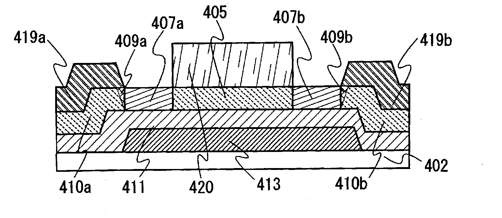
[0173]In FIG. 6A, a first electrode 313 and a sidewall insulating film 315 on side surfaces of the first electrode 313 are provided over an oxide semiconductor film 303. Further, a second electrode 319a and a third electrode 319b are in contact with bottom surfaces of third regions 309a and 309b in the oxide semiconductor film 303. The transistor 300 is a top-gate bottom-contact transistor.

[0174]FIG...


PUM


Abstract

A semiconductor device in which fluctuation in electric characteristics due to miniaturization is less likely to be caused is provided. The semiconductor device includes an oxide semiconductor film including a first region, a pair of second regions in contact with side surfaces of the first region, and a pair of third regions in contact with side surfaces of the pair of second regions; a gate insulating film provided over the oxide semiconductor film; and a first electrode that is over the gate insulating film and overlaps with the first region. The first region is a CAAC oxide semiconductor region. The pair of second regions and the pair of third regions are each an amorphous oxide semiconductor region containing a dopant. The dopant concentration of the pair of third regions is higher than the dopant concentration of the pair of second regions.

Description

TECHNICAL FIELD[0001]The present invention relates to a semiconductor device including an oxide semiconductor and method for manufacturing a semiconductor device.[0002]In this specification, the semiconductor device refers to all devices that can function by utilizing semiconductor characteristics. A transistor in this specification is a semiconductor device, and an electrooptic device, a semiconductor circuit, and an electronic device including the transistor are all semiconductor devices.BACKGROUND ART[0003]Transistors used for most flat panel displays typified by a liquid crystal display device and a light-emitting display device are formed using silicon semiconductors such as amorphous silicon, single crystal silicon, and polycrystalline silicon provided over glass substrates. Further, transistors formed using such silicon semiconductors are used in integrated circuits (ICs) and the like.[0004]Attention has been directed to a technique in which, instead of the above silicon semi...

Claims


Application Information

Patent Timeline
IPC IPC(8): H01L29/78H01L21/34
CPCH01L21/02554H01L21/02565H01L29/66969H01L29/7869H01L27/1203H01L21/02631H01L21/426H01L27/1225H01L27/1229H01L29/04H01L29/0847H01L29/36H01L29/42364H01L29/42384H01L29/4908H01L29/78621H01L29/78696
Inventor YAMAZAKI, SHUNPEI
Owner SEMICON ENERGY LAB CO LTD
Why Eureka
Try Eureka