Dram cell utilizing a doubly gated vertical channel

a vertical channel and dram technology, applied in the direction of semiconductor devices, electrical equipment, transistors, etc., can solve the problems of difficult scaling to very short channel lengths, large cell size of dg-ram, and more expensive soi substrates, and achieve the effect of low cos

Inactive Publication Date: 2012-06-28
RGT UNIV OF CALIFORNIA
View PDF5 Cites 14 Cited by
  • Summary
  • Abstract
  • Description
  • Claims
  • Application Information

AI Technical Summary

Benefits of technology

[0027]A still further element of the invention is the ability to fabricate the device in

Problems solved by technology

The silicon-on-insulator (SOI) floating body cell (FBC) design was offered as a 4F2 cell (having a cell area of 4F2), but required more expensive SOI substrates, and was difficult to scale to very short channe

Method used


Image

  • Dram cell utilizing a doubly gated vertical channel
  • Dram cell utilizing a doubly gated vertical channel
  • Dram cell utilizing a doubly gated vertical channel

Examples


embodiment 1

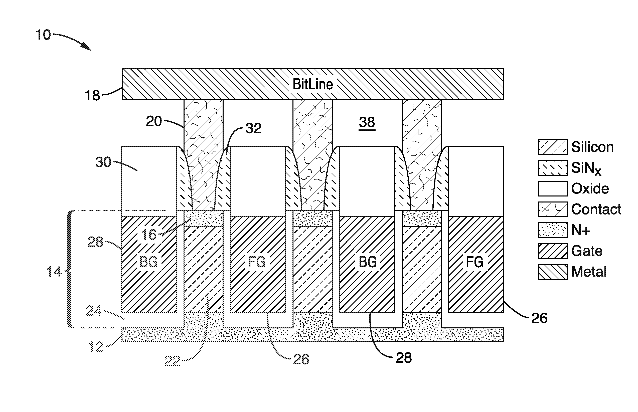
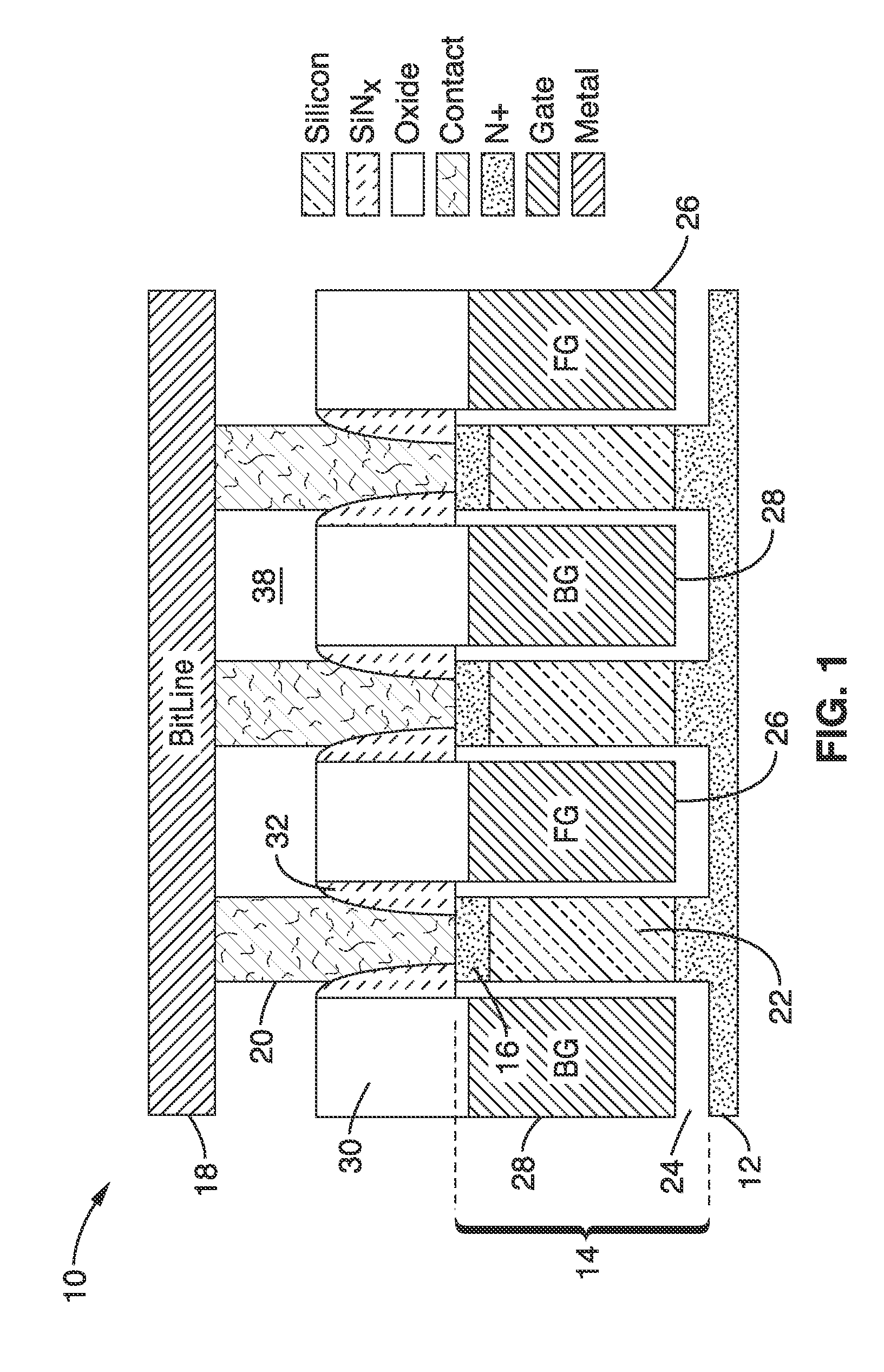
[0071]2. The DGVC memory cell array of embodiment 1, wherein said DGVC cell is configured without the need of charge storage capacitors separate from said plurality of double-gate transistor cells.

[0072]3. The DGVC memory cell array of embodiment 1, wherein said first end of said vertical channel is at the bottom of said vertical channel, while said second end of said vertical channel is at the top of said vertical channel.

[0073]4. The DGVC memory cell array of embodiment 1, wherein said first end of said vertical channel is at the top of said vertical channel, while said second end of said vertical channel is at the bottom of said vertical channel.

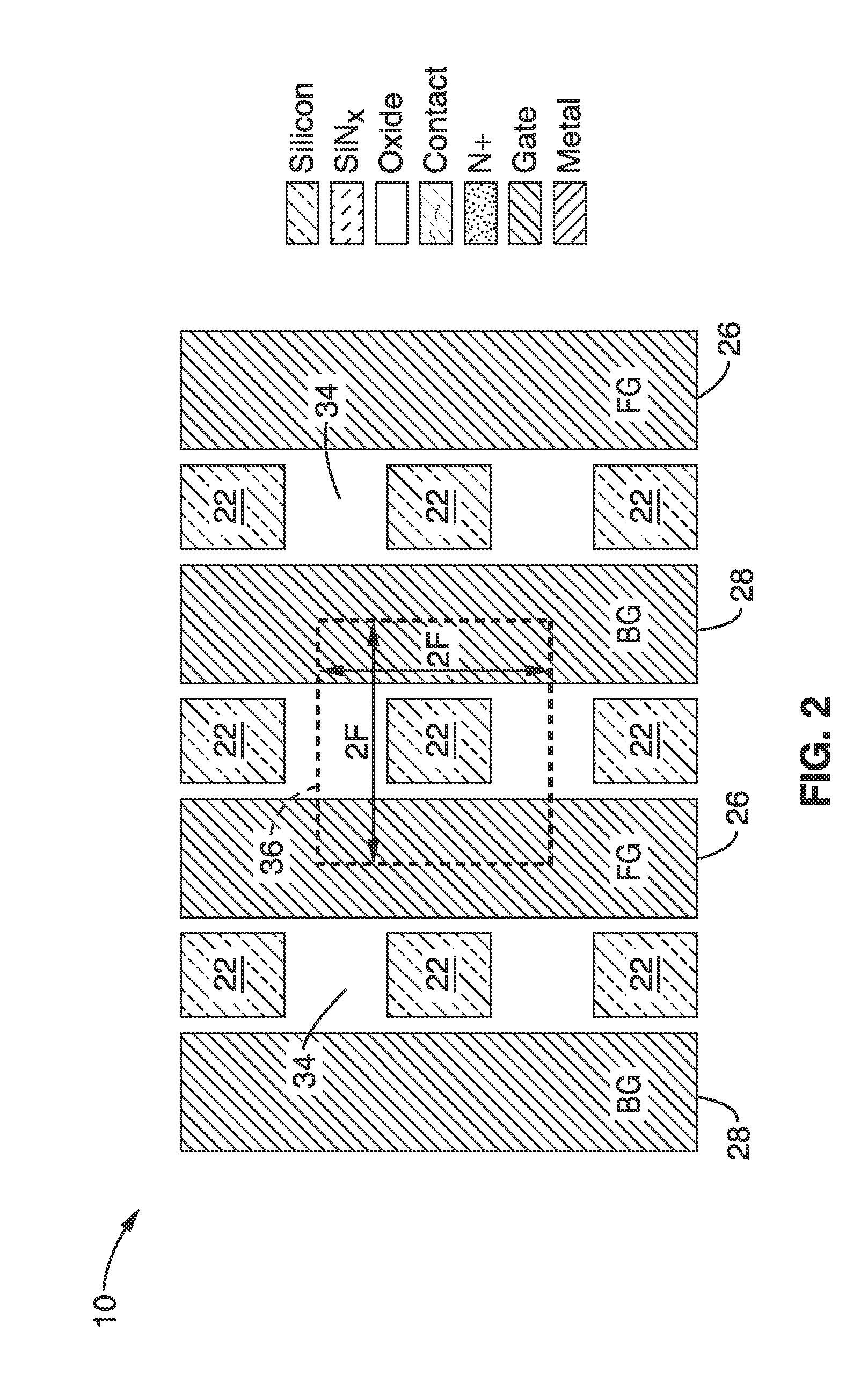
[0074]5. The DGVC memory cell array of embodiment 1, wherein the cell layout has length 2F on each side, so that it covers an area of 4F2, (thus a 4F2 cell) in which F represents the minimum lithographically-defined feature size of a fabrication process technology in which said double-gate vertical channel (DGVC) cell array is fabricated....

embodiment 6

[0076]7. The DGVC memory cell array of embodiment 6, wherein said semiconductor material is silicon (Si), or silicon-germanium (SiGe).

[0077]8. The DGVC memory cell array of embodiment 1, wherein said bit lines and gate lines comprise electrically conductive materials.

[0078]9. The DGVC memory cell array of embodiment 1, wherein said DGVC cell array further comprises: a back channel interface of a body region of the DGVC memory cell which accumulates holes in response to impact ionization during a Write “1” operation and which are removed through the drain junction during a Write “0” operation; wherein hole storage in the body region lowers threshold voltage which increases drain current during said Read operation; wherein a “1” or “0” state of a DGVC memory cell is determined in response to how much drain current is sensed during a Read operation.

[0079]10. A memory circuit, comprising: a plurality of memory cells; a double-gate vertical transistor structure within each memory cell; a...

embodiment 10

[0080]11. The memory circuit of embodiment 10, wherein said plurality of memory cells comprises a plurality of double-gate vertical transistor structures with channels positioned in gate facing orientations between the front and back gates.

[0081]12. The memory circuit of embodiment 10, wherein said source region is disposed at a common source region at a first end of the vertical channels which is shared by each said double-gate vertical transistor structure within said memory circuit; and wherein each said bit line is coupled to said drain region of each cell along the bit line direction at a second end of the vertical channels.


PUM


Abstract

A double-gate vertical channel transistor (DGVC) structure is described which is particularly well suited for Dynamic RAM (DRAM) memory (e.g., capacitorless DRAM) wherein the memory cell occupies a small cell area of 4F2, and provides beneficial retention properties including immunity to disturbances. The vertical transistors are arranged in an alternating gate-facing orientation, with a common source formed on a first end and separate drains on their second ends. Word lines comprise alternating front gates and back gates shared by columns of gate-facing transistors on each side of it. The DGVC cell provides enhanced scalability allowing the continued scaling of DRAM technology and can be fabricated using low-cost semiconductor materials and existing fabrication techniques. Fabrication techniques and array biasing are also described for the DGVC cell arrays.

Description

CROSS-REFERENCE TO RELATED APPLICATIONS[0001]This application a 35 U.S.C. §111(a) continuation of PCT international application number PCT / US2010 / 048116 filed on Sep. 8, 2010, incorporated herein by reference in its entirety, which is a nonprovisional of U.S. provisional patent application Ser. No. 61 / 240,341 filed on Sep. 8, 2009, which is incorporated herein by reference in its entirety. Priority is claimed to each of the foregoing applications.[0002]The above-referenced PCT international application was published as PCT International Publication No. WO 2011 / 031749 on Mar. 17, 2011 and republished on May 19, 2011, and is incorporated herein by reference in its entirety.STATEMENT REGARDING FEDERALLY SPONSORED RESEARCH OR DEVELOPMENT[0003]Not ApplicableINCORPORATION-BY-REFERENCE OF MATERIAL SUBMITTED ON A COMPACT DISC[0004]Not ApplicableNOTICE OF MATERIAL SUBJECT TO COPYRIGHT PROTECTION[0005]A portion of the material in this patent document is subject to copyright protection under t...

Claims


Application Information

Patent Timeline
IPC IPC(8): H01L29/78H01L21/336
CPCH01L27/108H01L27/10802H01L29/7841H01L29/7827H01L27/10876H10B12/20H10B12/053H10B12/00
Inventor KWON, WOOKHYUNLIU, TSU-JAE KING
Owner RGT UNIV OF CALIFORNIA
Why Eureka
Try Eureka