Method for forming nitride film

a technology of nitride film and nitride film, which is applied in the direction of coating, chemical vapor deposition coating, metallic material coating process, etc., can solve the problems of increasing the resistance of the wiring, nitriding of the surface of the w wiring, and deteriorating the adhesion strength of the wiring, so as to prevent the uniform thickness of the film and suppress the loading effect

Inactive Publication Date: 2012-06-28
ELPIDA MEMORY INC +1
View PDF4 Cites 35 Cited by
  • Summary
  • Abstract
  • Description
  • Claims
  • Application Information

AI Technical Summary

Benefits of technology

[0017]As a result of intensive studies on a solution for preventing the uniformity in the film thickness on the wafers in a furnace bottom portion from being deteriorated due to the loading effect in the plasma-assisted ALD process using the batch-type vertical furnace, the inventors have found that an influence of the loading effect can be suppressed by varying flow rates of the carrier gases between the introducing of the DCS gas and the introducing of the ammonia gas.
[0024]According to the invention, a sufficient production amount of the radical can be also obtained in the bottom portion of the furnace, and hence, providing an improvement to the film thinning phenomenon due to the loading effect on the center portion of the wafer.

Problems solved by technology

As a result, there are problems that the resistance of the wiring is increased and also the adhesion strength of the wiring is deteriorated due to the volume expansion thereof, etc.
However, the formation of the silicon nitride film by the CVD process causes a nitriding of the surface of the W wiring.
Thus nitrided tungsten (WN) still maintains electric conductivity, but compared with tungsten (W), the resistance value thereof is approximately 10 times higher, and hence there is a problem that a wiring having a sufficiently low resistance for a micro wiring cannot be obtained.
Because of the reduction of the N radial at the bottom portion, an amount of the N radical reaching to a center portion of the wafer is reduced and therefore DCS is insufficiently nitrided.
In particular, because, as a surface area of a pattern is become larger, a more amount of the radical will be consumed, and hence, the film thickness on the center portion of the water is easily reduced (hereafter, referred to as “a film thinning phenomenon”), leading to a problem that a uniformity in the film thickness within a wafer surface is deteriorated (due to a loading effect).
In order to solve such a problem, a technique in which the wafer is not placed on boats of the bottom portion is considered, and rather leading to a problem that productivity is deteriorated.

Method used


Image

  • Method for forming nitride film
  • Method for forming nitride film
  • Method for forming nitride film

Examples


Embodiment Construction

[0033]The invention will be now described herein with reference to illustrative embodiments. Those skilled in the art will recognize that many alternative embodiments can be accomplished using the teachings of the invention and that the invention is not limited to the embodiments illustrated for explanatory purpose.

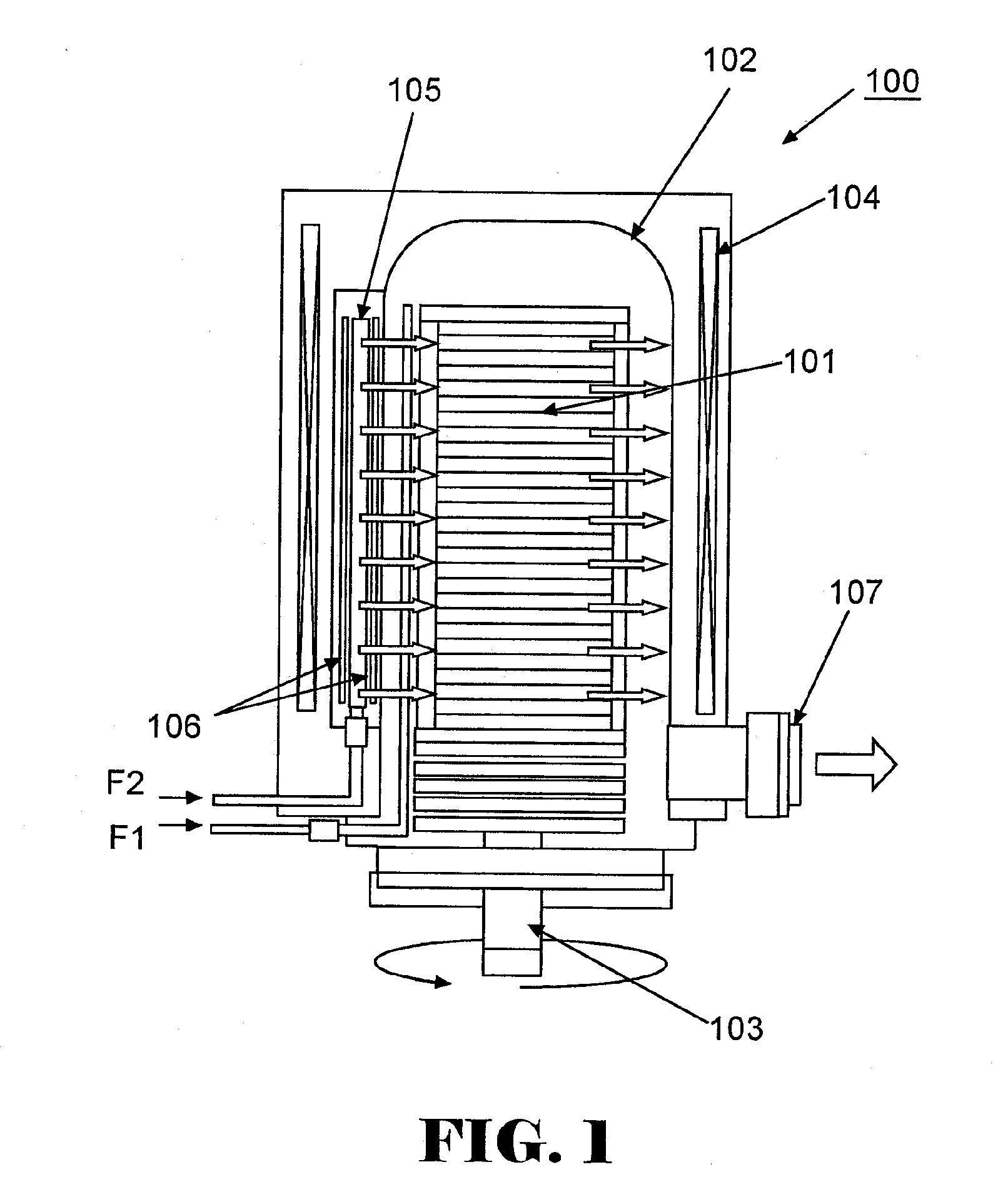
[0034]In an embodiment below, a method for forming a silicon nitride film on word lines being become into gate electrodes formed in a line shape, in particular, gate electrodes of a MOS transistor serving as an active device in memory cells of DRAM, will be explained.

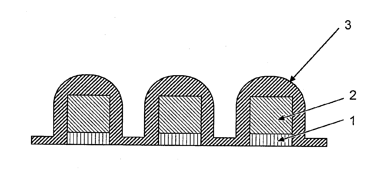
[0035]In a transistor formation region as shown in FIG. 3, a gate insulating film (not shown) made of a silicon oxide film is formed on a surface of the semiconductor substrate, for example, by a thermal oxidation method and the like.

[0036]A gate electrode 1 composed of a multilayer film comprising, for example, a polysilicon film and a metal film, is formed on the gate insulating film. As the polysilicon fil...


PUM

PropertyMeasurementUnit
temperatureaaaaaaaaaa

Abstract

A plasma-assisted ALD method using a vertical furnace and being performed by repeating a cycle until a desired film thickness is obtained is disclosed. The cycle comprises introducing a source gas containing a source to be nitrided, adsorbing, purging, introducing a nitriding gas and nitriding the source, and then, purging. A flow rate of a second carrier gas during introduction of the nitriding gas is reduced relative to that of a first carrier gas during introduction of the source gas. Particularly, a flow ratio of NH3 gas as the nitriding gas to N2 gas as the second carrier gas is 50:3 or less.

Description

BACKGROUND OF THE INVENTION[0001]1. Field of the Invention[0002]The invention relates to a method for forming a nitride film, and more particularly to a method for forming a nitride film on a semiconductor wafer having a high density pattern formed thereon, using a batch-type vertical plasma-assisted ALD (Atomic Layer Deposition) apparatus.[0003]2. Description of the Related Art[0004]In semiconductor devices, tungsten (W), a refractory metal, has been generally used as a wiring in portions where heat resistance is required.[0005]Also, in semiconductor devices having multi-layer wiring structures, an interlayer dielectric film is formed to electrically insulate the wiring of each layer from one another, but as the interlayer dielectric film, a silicon oxide film formed by CVD (Chemical Vapor Deposition) process is used.[0006]Tungsten (W) is easily oxidized in an oxygen atmosphere during formation of a silicon oxide film, and thereby produces tungsten oxide (WOx) having a much higher ...

Claims


Application Information

Patent Timeline
Patent Type & Authority Applications(United States)
IPC IPC(8): H01L21/318
CPCC23C16/345C23C16/45542C23C16/45578H01L21/76834H01L21/02211H01L21/02274H01L21/0228H01L21/0217H01L21/0254
Inventor FUJII, MOTOKIMATSUNAGA, MASANOBUYAMAMOTO, KAZUYAUMEZAWA, KOTA
Owner ELPIDA MEMORY INC
Why Eureka
Try Eureka