
Selective metalization of electrical connector or socket housing

Active Publication Date: 2012-07-05
HSIO TECH
View PDF5 Cites 65 Cited by
  • Summary
  • Abstract
  • Description
  • Claims
  • Application Information

AI Technical Summary

Benefits of technology

[0012]The contact members rely on known spring properties and solder joint methods. The layers structure of the housing eliminates the need for contact retention features, greatly reducing the complexity of the component and the tooling required to produce them. In some embodiments, the present interconnect eliminates the need to add solder balls to the assembly, reducing cost and eliminating at least one reflow cycle which can warp or damage the socket. The interconnect can also reduce or redistribute the terminal pitch without the addition of an interposer or daughter substrate.
[0018]The use of additive printing processes permits the material set in a given layer to vary. Traditional PCB and flex circuit fabrication methods take sheets of material and stack them up, laminate, and / or drill. The materials in each layer are limited to the materials in a particular sheet. Additive printing technologies permit a wide variety of materials to be applied on a layer with a registration relative to the features of the previous layer. Selective addition of conductive, non-conductive, or semi-conductive materials at precise locations to create a desired effect has the major advantages in tuning impedance or adding electrical function on a given layer. Tuning performance on a layer by layer basis relative to the previous layer greatly enhances electrical performance.

Problems solved by technology

As IC devices advance to next generation architectures traditional IC sockets have reached mechanical and electrical limitations that require alternate methods.
Longer contact members also tend to reduce signal integrity and increase contact resistance due to self-heating of power delivering contacts.
The thinner insulating walls increase the difficulty of molding and increase latent stresses in the IC socket housing, increasing the risk of warpage during solder reflow.
The thinner insulating walls also increase the risk of cross-talk between adjacent contact members.
Traditional IC sockets have reached an electrical performance limit.
Next generation IC devices will operate above 5 GHz and beyond and the existing IC sockets do not provide acceptable performance levels without significant revision.
A major issue with the use of spring probes in test sockets is the electrical performance is degraded by the coil spring which is an inductor, as well as the potential capacitance of the metal members and the relatively high contact resistance due to the various sliding connection point.

Method used


Image

  • Selective metalization of electrical connector or socket housing
  • Selective metalization of electrical connector or socket housing
  • Selective metalization of electrical connector or socket housing

Examples


Embodiment Construction

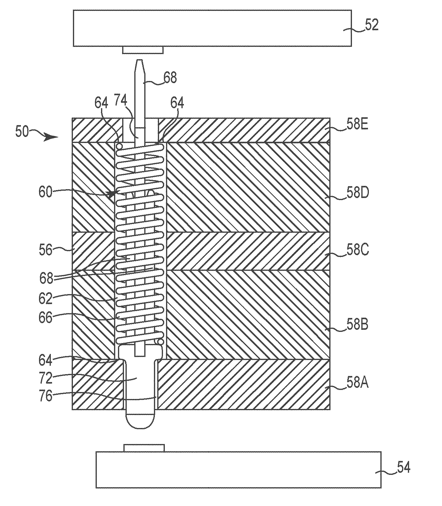
[0047]A high performance electrical interconnect according to the present disclosure may permit fine contact-to-contact spacing (pitch) on the order of less than 1.0 mm pitch, and more preferably a pitch of less than about 0.7 millimeter, and most preferably a pitch of less than about 0.4 millimeter. Such fine pitch high performance electrical interconnects are especially useful for communications, wireless, and memory devices.

[0048]The present high performance electrical interconnect can be configured as a low cost, high signal performance interconnect assembly, which has a low profile that is particularly useful for desktop and mobile PC applications. IC devices can be installed and uninstalled without the need to reflow solder. The solder-free electrical connection of the IC devices is environmentally friendly.

[0049]FIG. 1 is a sectional view of an electrical interconnect 50 that provides an interface between IC device 52 and PCB 54 in accordance with an embodiment of the present...


PUM

PropertyMeasurementUnit
Dielectric polarization enthalpyaaaaaaaaaa
Flexibilityaaaaaaaaaa
Moldableaaaaaaaaaa

Abstract

A electrical interconnect adapted to provide an interface between contact pads on an IC device and a PCB. The electrical interconnect includes a multi-layered substrate with a first surface with a plurality of first openings having first cross-sections, a second surface with a plurality of second openings having second cross-sections, and center openings connecting the first and second openings. The center openings include at least one cross-section greater than the first and second cross-sections. A plurality of spring probe contact members are located in the center openings. The contact members include first contact tips extending through the first opening and above the first surface, second contact tips extending through the second openings and above the second surface, and center portions located in the center openings. The center portions include a shape adapted to bias the first and second contact tips toward the IC device and PCB, respectively. A dielectric material different from the material of the substrate is located in at least one of the first opening, the second opening, or the center opening.

Description

[0001]This application claims the benefit of U.S. Provisional Application No. 61 / 449,889, filed Mar. 7, 2011, the disclosure of which is hereby incorporated by reference.[0002]The present application is a continuation-in-part of International Application No. PCT / US2011 / 038845, titled Electrical Connector Insulator Housing, filed Jun. 2, 2011, which claims the benefit of U.S. Provisional Application No. 61 / 351,114, entitled Electrical Connector Insulator Housing, filed Jun. 3, 2010, which are hereby incorporated by reference in their entireties.[0003]The present application is a continuation-in-part of International Application No. PCT / US2011 / 062313, titled HIGH PERFORMANCE SURFACE MOUNT ELECTRICAL INTERCONNECT, filed Nov. 29, 2011, which claims the benefit of U.S. Provisional Application No. 61 / 418,625, filed Dec. 1, 2010, which are hereby incorporated by reference in their entireties.TECHNICAL FIELD[0004]The present disclosure relates to an electrical interconnect between an integr...

Claims


Application Information

Patent Timeline
IPC IPC(8): H01R13/24H01R43/16
CPCH05K2201/10378H05K1/023H05K1/16H01R12/57H01R12/523H01R12/716Y10T29/49204H01R12/52H05K1/141H01R13/2421H05K3/4007
Inventor RATHBURN, JAMES
Owner HSIO TECH
Features
  • Generate Ideas
  • Intellectual Property
  • Life Sciences
  • Materials
  • Tech Scout
  • Unparalleled Data Quality
  • Higher Quality Content
  • 60% Fewer Hallucinations
Learn More