Semiconductor memory device

a memory device and semiconductor technology, applied in the direction of semiconductor devices, electrical devices, transistors, etc., can solve the problems of difficult to form a capacitor having a sufficient capacitance, burdening circuit design and device characteristics, and reducing the integration degree of the open-bit-line dram, so as to achieve suppress the short-channel effect, the effect of reducing the integration degree and reducing the channel length

Inactive Publication Date: 2012-08-02
SEMICON ENERGY LAB CO LTD
View PDF16 Cites 29 Cited by
  • Summary
  • Abstract
  • Description
  • Claims
  • Application Information

AI Technical Summary

Benefits of technology

[0024]Note that in the case where the word line is provided at the side surface of the recessed portion or the projected portion, a channel length of the transistor whose gate is formed using the word line is substantially equal to the height of the side surface or the depth of the recessed portion or the projected portion. Therefore, for example, when such a height or depth is appropriately determined, the integration degree is not reduced, the channel length can be larger than the feature size, and a short-channel effect can be suppressed.
[0025]In addition, in the above structure, the bit line is located in a position apart from the capacitor and the word line, and thus, a parasitic capacitance between the bit line and the capacitor or the word line can be reduced. When the parasitic capacitance of the bit line is reduced, the capacitance of the capacitor provided in a memory cell can be reduced in proportion thereto.
[0026]Note that in the above structure, since the bit line is located below the transistor and there is no structure that becomes an obstruction, the depth at which the bit line is provided can be arbitrarily determined. Needless to say, the formation of the bit line in a position apart from another wiring makes it possible to further reduce the parasitic capacitance. In addition, when the depths of the bit lines adjacent to each other are different from each other, a parasitic capacitance between the adjacent bit lines can also be reduced.
[0027]Further, when a circuit for driving a memory array is provided below the memory cell array, the area of a chip can be reduced. The area of a driver circuit occupies 20% to 50% of the area of a surface of a usual DRAM chip. When the driver circuit and the memory cell array are provided to overlap with each other, the area of the chip can be reduced, and a larger number of memory cells can be formed compared to the case of the usual DRAM chip having the same area.

Problems solved by technology

Manufacturing of an open-bit-line DRAM using a stacked capacitor method is a burden on a circuit design and device characteristics.
However, in a memory cell which is particularly miniaturized, it has been difficult to form a capacitor having a sufficient capacitance.

Method used


Image

  • Semiconductor memory device
  • Semiconductor memory device
  • Semiconductor memory device

Examples


embodiment 1

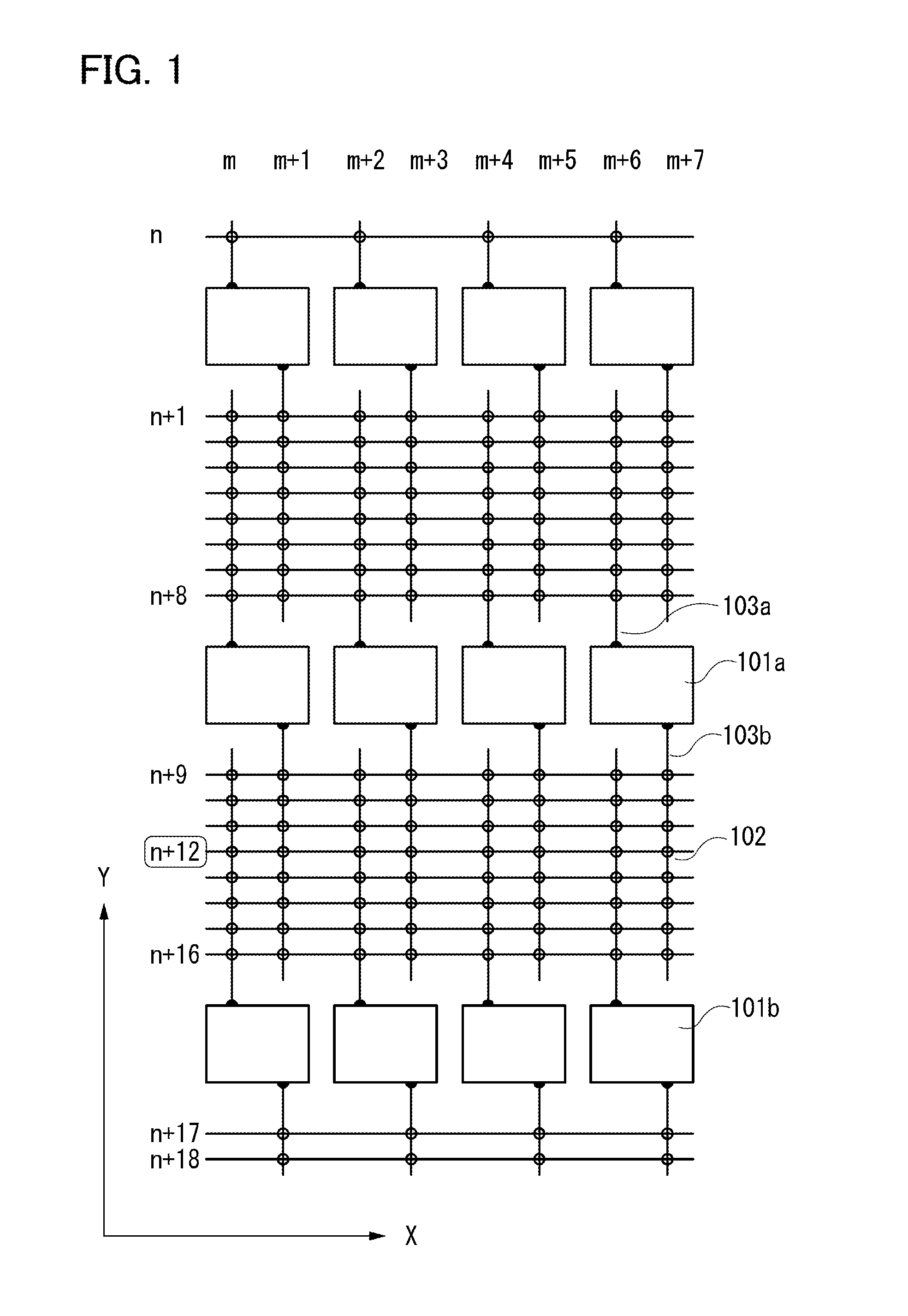
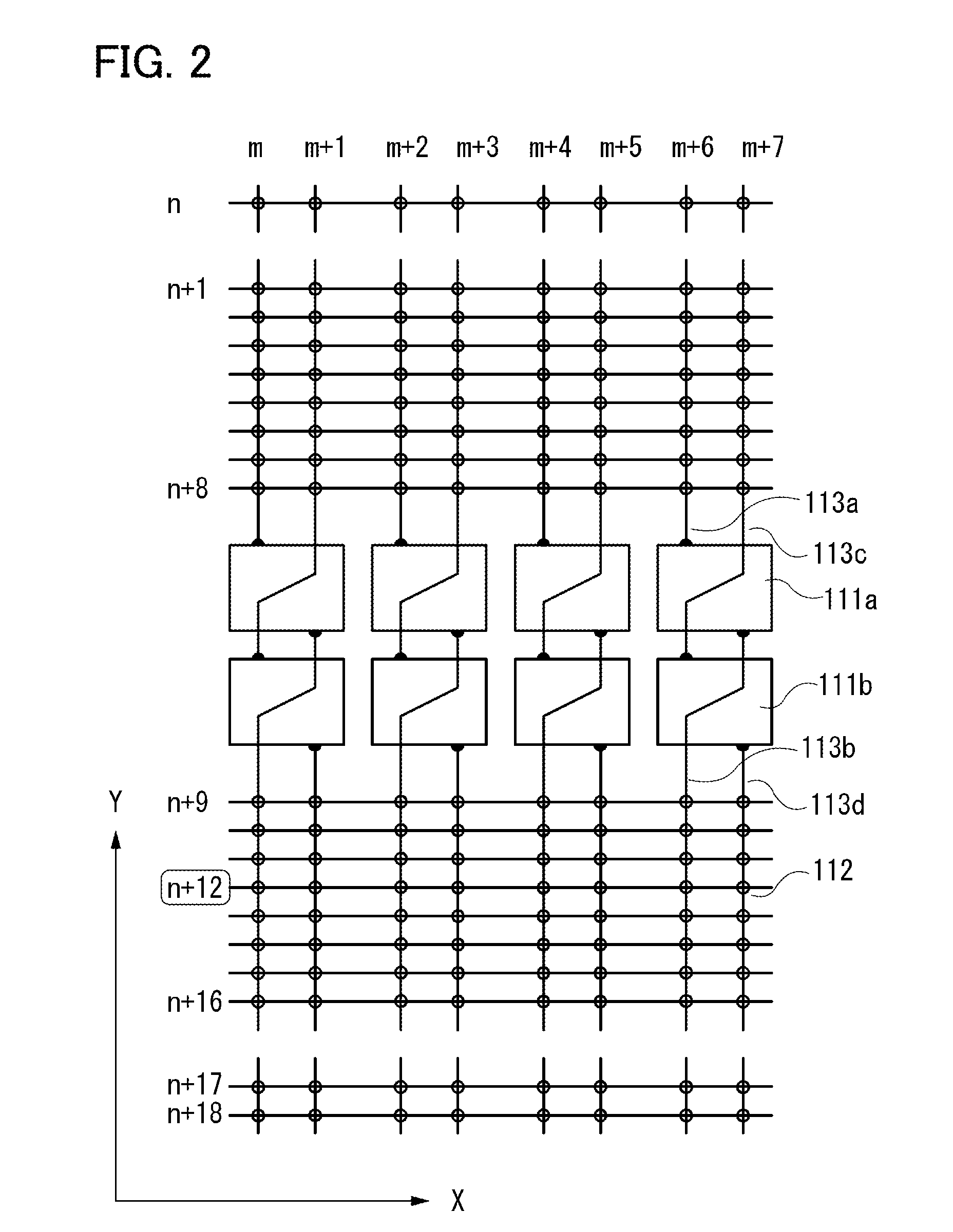
[0039]FIG. 1 and FIG. 2 each illustrate an example of circuit arrangement of a DRAM to which the present invention is applied. In FIG. 1 and FIG. 2, lines extending in a Y direction indicate bit lines and m to (m+7) columns are illustrated. Further, in FIG. 1 and FIG. 2, lines extending in an X direction indicate word lines and n to (n+18) rows are illustrated. Furthermore, in FIG. 1 and FIG. 2, circles located on intersections of lines indicate memory cells and rectangles each connected to one end of the line indicate sense amplifiers.

[0040]FIG. 1 illustrates circuit arrangement called a relaxed-open-bit-line type in open-bit-line DRAMs. Bit lines 103a and 103b connected to a sense amplifier 101a are provided to extend upward and downward in the drawing, respectively, from the sense amplifier 101a.

[0041]For example, in order to read data of a memory cell 102 in the (n+12) row and the (m+7) column, the following operations are performed: the word line in the (n+12) row is activated...

embodiment 2

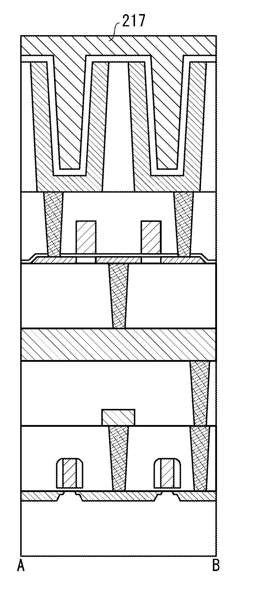
[0087]FIGS. 7A to 7D and FIGS. 8A to 8D illustrate this embodiment. Although in this embodiment, a memory cell is formed over a semiconductor circuit including a sense amplifier as in Embodiment 1, the semiconductor circuit is omitted in FIGS. 7A to 7D and FIGS. 8A to 8D. Description is made below with reference to the drawings.

7A>

[0088]A bit line 402 is formed over a first insulator 401. At this time, there are some methods of arrangement of the bit line 402. For example, there is a method in which, as illustrated in FIGS. 8A and 8B, the bit line 402 and adjacent bit lines 402a and 402b are formed at the same depth or formed in the same layer. FIG. 8A is a schematic view of a cross section of a surface where the bit line 402 is formed, which is taken along a plane through line C-D of FIG. 7A, and FIG. 8B illustrates a cross section taken along line E-F of FIG. 8A. Note that cross sections along lines A-B of FIGS. 8A and 8C are illustrated in FIGS. 7A to 7D.

[0089]As illustrated in F...


PUM


Abstract

A highly integrated DRAM is provided. A circuit for driving a memory cell array is formed over a substrate, a bit line is formed thereover, and a semiconductor region, word lines, and a capacitor are formed over the bit line. Since the bit line is located below the semiconductor region, and the word lines and the capacitor are located above the semiconductor region, the degree of freedom of the arrangement of the bit line is high. When an open-bit-line DRAM is formed, an area per memory cell less than or equal to 6F2, or when a special structure is employed for a cell transistor, an area per memory cell less than or equal to 4F2 can be achieved.

Description

BACKGROUND OF THE INVENTION[0001]1. Field of the Invention[0002]The present invention relates to a semiconductor memory device.[0003]2. Description of the Related Art[0004]Dynamic random access memories (DRAMs) are widely used as typical semiconductor memory devices. DRAMs are divided into two kinds of DRAMs by the difference in signal detecting method of bit lines, that is, open-bit-line DRAMs and folded-bit-line DRAMs (for example, see Patent Document 1).[0005]In the folded-bit-line DRAM, memory cells are provided in half of all intersections of word lines and bit lines, and thus the area per memory cell is greater than or equal to 8F2 (F is a feature size). In contrast, in the open-bit-line DRAM, ideally, a contact can be shared, and thus the area per memory cell can be reduced to 6F2.[0006]In addition, as a formation method of a capacitor in a DRAM, two kinds of formation methods, that is, a trench capacitor method in which a deep hole is formed in a silicon substrate, and a sta...

Claims


Application Information

Patent Timeline
Patent Type & Authority Applications(United States)
IPC IPC(8): H01L27/108
CPCH01L27/0207H01L27/10891H01L27/10885H01L27/10814H10B12/315H10B12/488H10B12/482H01L21/76877H10B12/31
Inventor TAKEMURA, YASUHIKO
Owner SEMICON ENERGY LAB CO LTD
Why Eureka
Try Eureka