Manufacturing method for an optical waveguide and optical waveguide body used therefor

a technology of optical waveguides and manufacturing methods, applied in the direction of instruments, cladded optical fibres, optical elements, etc., can solve the problems of poor visibility of marks, inability to achieve efficient optical connection at the coupled portion, and difficult recognition, so as to achieve sufficient cut position accuracy, improve visibility, and reduce the effect of refractive index

Inactive Publication Date: 2012-08-02
NITTO DENKO CORP
View PDF6 Cites 6 Cited by
  • Summary
  • Abstract
  • Description
  • Claims
  • Application Information

AI Technical Summary

Benefits of technology

[0010]A manufacturing method for an optical waveguide and an optical waveguide body used therefor are provided in which, when an optical waveguide is cut and a contour thereof is processed, accuracy of a cut position is improved by improving visibility of an alignment mark.
[0013]Specifically, after a core and an alignment mark were formed on an undercladding layer, an overcladding layer was formed so as to cover the core with the alignment mark being exposed, unlike a conventional case in which an alignment mark was, together with a core, formed within a cladding layer so as to be embedded therein. When the cut position is located with reference to the alignment mark from a rear surface side of the undercladding layer which is formed with the alignment mark being exposed in this way, the alignment mark is not covered with the overcladding layer but is exposed, and thus, the difference in refractive index between the alignment mark and the surroundings (air) becomes larger. Further, not a rounded portion of an upper portion of the alignment mark but a lower portion of the alignment mark at which the border is distinct is viewed. Therefore, the visibility is improved, and sufficient accuracy of the cut position may be secured. The above-mentioned undercladding layer and overcladding layer were able to be cut at a predetermined position with high accuracy.
[0014]As described above, a manufacturing method for an optical waveguide is provided by, after forming, on an undercladding layer, an overcladding layer so as to cover a core pattern with an alignment mark being exposed, locating a cut position from a rear surface side of the undercladding layer with reference to the alignment mark, and cutting the undercladding layer and the overcladding layer at a predetermined position. An optical waveguide body used for the manufacturing method for an optical waveguide is provided, including an undercladding layer, a core formed on the undercladding layer, an overcladding layer formed so as to cover the core, and an alignment mark formed on the undercladding layer so that a front surface thereof is exposed without being covered with the overcladding layer. Therefore, the visibility of the alignment mark is improved, and the positional accuracy when the cut position is located with reference to the alignment mark is significantly improved. This results in improvement of the production yield of the optical waveguide to obtain an optical waveguide which is excellent in productivity and reliability.

Problems solved by technology

Here, if the contour of the optical waveguide and a core in the optical waveguide are misaligned, efficient optical connection cannot be achieved at the coupled portion.
The difference in refractive index between the mark and the overcladding layer is small, and thus, there is a problem that the mark has poor visibility.
In particular, when the above-mentioned mark which is formed together with the core is visually recognized using an image analyzer or the like, the recognition is very difficult.
Even if the recognition is possible, it is difficult to secure sufficient accuracy.
However, in the method described in Japanese Patent Application Laid-open No. 2010-72435, the mark for setting the position is formed and fixed on the surface of the optical waveguide main body, and thus, there is a problem that misalignment occurs when the mark is fixed.
The misalignment accumulates as an error when the cutting is carried out, and thus, even if the visibility of the mark is improved, it is difficult to, as a result, secure positional accuracy for the cutting which is sufficiently satisfactory.

Method used


Image

  • Manufacturing method for an optical waveguide and optical waveguide body used therefor
  • Manufacturing method for an optical waveguide and optical waveguide body used therefor
  • Manufacturing method for an optical waveguide and optical waveguide body used therefor

Examples


example 1

Formation of Undercladding Layer

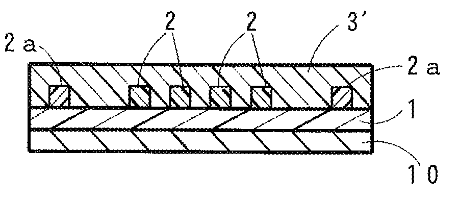
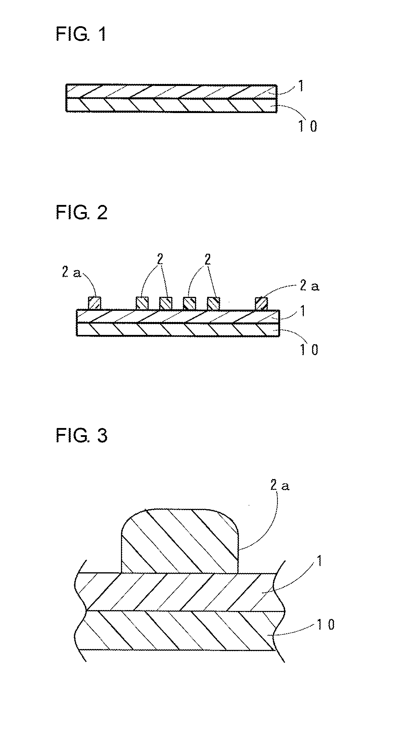
[0051]The above-mentioned undercladding layer forming material (varnish) was applied to a front surface of a substrate formed of glass (manufactured by Central Glass Co., Ltd., 140 mm×140 mm×thickness 1.1 mm) using a spin coater (1X-DX2 manufactured by MIKASA CO., LTD.). After that, drying treatment at 130° C. for 10 minutes was carried out in a drying oven to form an applied layer (undercladding layer before being cured). Then, an exposure machine (MA-60A manufactured by MIKASA CO., LTD.) and an ultra high pressure mercury-vapor lamp (USH-250D manufactured by USHIO INC.) were used to apply an ultraviolet ray (having a wavelength of 365 nm) to the entire front surface of the undercladding layer before being cured to carry out exposure so that the accumulated light quantity was 2,000 mJ / cm2. Then, heating treatment at 130° C. for 10 minutes was carried out to manufacture the undercladding layer (having a thickness of 25 μm) (see FIG. 1).

(Formation of C...


PUM


Abstract

Provided is a manufacturing method for an optical waveguide in which, when the optical waveguide is cut and a contour thereof is processed, accuracy of a cut position is improved by improving visibility of an alignment mark. An undercladding layer, cores, and alignment marks are formed on a front surface of a substrate. Then, an overcladding layer is formed using a photomask so as to cover the cores with the alignment marks being exposed. After the substrate is separated to manufacture an optical waveguide body, a cut position is located with reference to the alignment marks from a rear surface side of the undercladding layer, and the undercladding layer and the overcladding layer are cut to manufacture the optical waveguide.

Description

BACKGROUND OF THE INVENTION[0001]1. Field of the Invention[0002]The present invention relates to a manufacturing method for an optical waveguide which is widely used in optical communication, optical information processing, position sensors, and other fields of general optics, and an optical waveguide body used therefor.[0003]2. Description of the Related Art[0004]In general, in signal transmission using optical wiring, an optical connector is used to couple optical fibers and / or optical waveguides. The optical connector includes a band-like optical waveguide, and a connection terminal having a predetermined shape called “ferrule”, which is mounted to a longitudinal end portion of the optical waveguide and has guide holes into which guide pins for alignment may be inserted. As such a ferrule, in general, a PMT ferrule described in JPCA Standards “Detail Specification for PMT Connector” (JPCA-PE03-01-07-(2006)) is often used. In an optical connector using such an optical waveguide, t...

Claims


Application Information

Patent Timeline
Patent Type & Authority Applications(United States)
IPC IPC(8): G02B6/02G02B6/10
CPCG02B6/138G02B6/1221
Inventor TSUJITA, YUICHITAKASE, MAYU
Owner NITTO DENKO CORP
Why Eureka
Try Eureka