Liquid crystal device comprising array of sensor circuits using a pre-charge operation

a liquid crystal device and sensor circuit technology, applied in the field of liquid crystal devices, can solve the problems of affecting the display quality, mechanical deformation of the liquid crystal cell, and the use of rows and columns for both display and sensing functions, so as to increase the sensitivity of the capacitance sensor array, and achieve the effect of reducing the mechanical integrity of the display

Inactive Publication Date: 2012-08-16
SHARP KK
View PDF0 Cites 15 Cited by
  • Summary
  • Abstract
  • Description
  • Claims
  • Application Information

AI Technical Summary

Benefits of technology

[0053]It is possible to increase the sensitivity of capacitance measurement in a capacitance sensor array. In particular, it is possible to increase the sensitivity of a capacitance sensor array comprising active pixel sensor circuits. Such techniques are applicable to capacitance sensor arrays in general and, more specifically, to capacitance sensor arrays integrated into liquid crystal displays in which the liquid crystal material is used both as the optical element of the display and as the dielectric of the capacitor to be measured.
[0054]The sensitivity of the active pixel sensor circuit to changes in capacitance of the variable liquid crystal capacitor may be increased relative to the prior art. The following advantages arise from this feature. Firstly, it is possible to integrate a force sensitive touch panel within an AMLCD without significantly compromising the mechanical integrity of the display. As a result, touching the display causes little or no degradation in the quality of the displayed image. Secondly, the ratio of the measured signal to the noise is increased resulting in a more accurate measurement of the force of touch and a more reliable and robust operation. Additionally, for simple touch panel applications, the cost of manufacture of the AMLCD may be reduced since the need for specific in-cell structures to increase the sensitivity of the sensor is obviated by the improved active pixel sensor circuit.
[0055]Another advantage arises in embodiments where the planar structure of the sensor electrodes forms the variable liquid crystal capacitor. Compared to the prior art in which one of the electrodes forming the variable liquid crystal capacitor was common with the display operation, such embodiments, provide two electrodes unique to the sensor operation. As a result, the sensor is less susceptible to electrical noise and interference from the display operation and the accuracy of the capacitance measurement, and hence accuracy of the touch force measurement, is increased.

Problems solved by technology

Whilst it is desirable on the part of the sensor for mechanical deformation to cause a large and easily detectable change in the liquid crystal cell, such a large change has a deleterious effect on the display quality.
In these devices, an input object—such as a finger or stylus—is used apply pressure to the surface of the display resulting in mechanical deformation of the liquid crystal cell.
A significant disadvantage of this arrangement however is that the rows and columns must be used for both the display and sensing functions.
However, a disadvantage common to all passive matrix type sensors is that the accuracy of the capacitance that can be measured is limited by the parasitic capacitance of the row and column addressing lines.
These parasitic elements attenuate the signal generated by the variable liquid crystal capacitance and make the sensor susceptible to interference and noise.
In addition, passive matrix sensors require external connections to be made to each row and column, thus increasing the cost and reducing the reliability of the device.
A disadvantage however is that the capacitance change corresponding to an input object touching the display is very small and difficult for the detection circuits of the sensor to measure accurately.
A disadvantage common to all passive pixel type sensors is that, especially for large arrays, the liquid crystal capacitor element is small compared to the parasitic capacitance of the addressing lines and the accuracy of the capacitance measurement therefore remains low.
Further, the measurement is easily affected by noise and interference from the display operation.
Although the active pixel type sensor provides a significantly more accurate measure of the liquid crystal capacitance than either the passive matrix or passive pixel types, in practice the sensitivity of the pixel output signal to changes in the capacitance of the liquid crystal capacitor elements associated with realistic mechanical deformations of the cell-gap remains too small.
However, since the display uses the same liquid crystal cell as the sensor, a serious side-effect of this approach is that the quality of the displayed image may be severely degraded in the region around where the input object touches the display.
Whilst these structures are helpful to improve the sensitivity of the capacitance sensor, there remains a mismatch between the change in capacitance that can be comfortably generated by the user pressing the input object on the display and that which is reliably detectable by the sensor.
In particular, this low sensitivity remains a problem when using input objects with a large contact area, such as a finger, where for a given input force a smaller pressure is generated than with an input object of smaller contact area, such as a stylus or pen.

Method used


Image

  • Liquid crystal device comprising array of sensor circuits using a pre-charge operation
  • Liquid crystal device comprising array of sensor circuits using a pre-charge operation
  • Liquid crystal device comprising array of sensor circuits using a pre-charge operation

Examples


first embodiment

[0094]This embodiment describes the basic concept whereby a voltage-dependent select capacitor is used to increase the sensitivity of the output of an active pixel sensor circuit to changes in the liquid crystal capacitance.

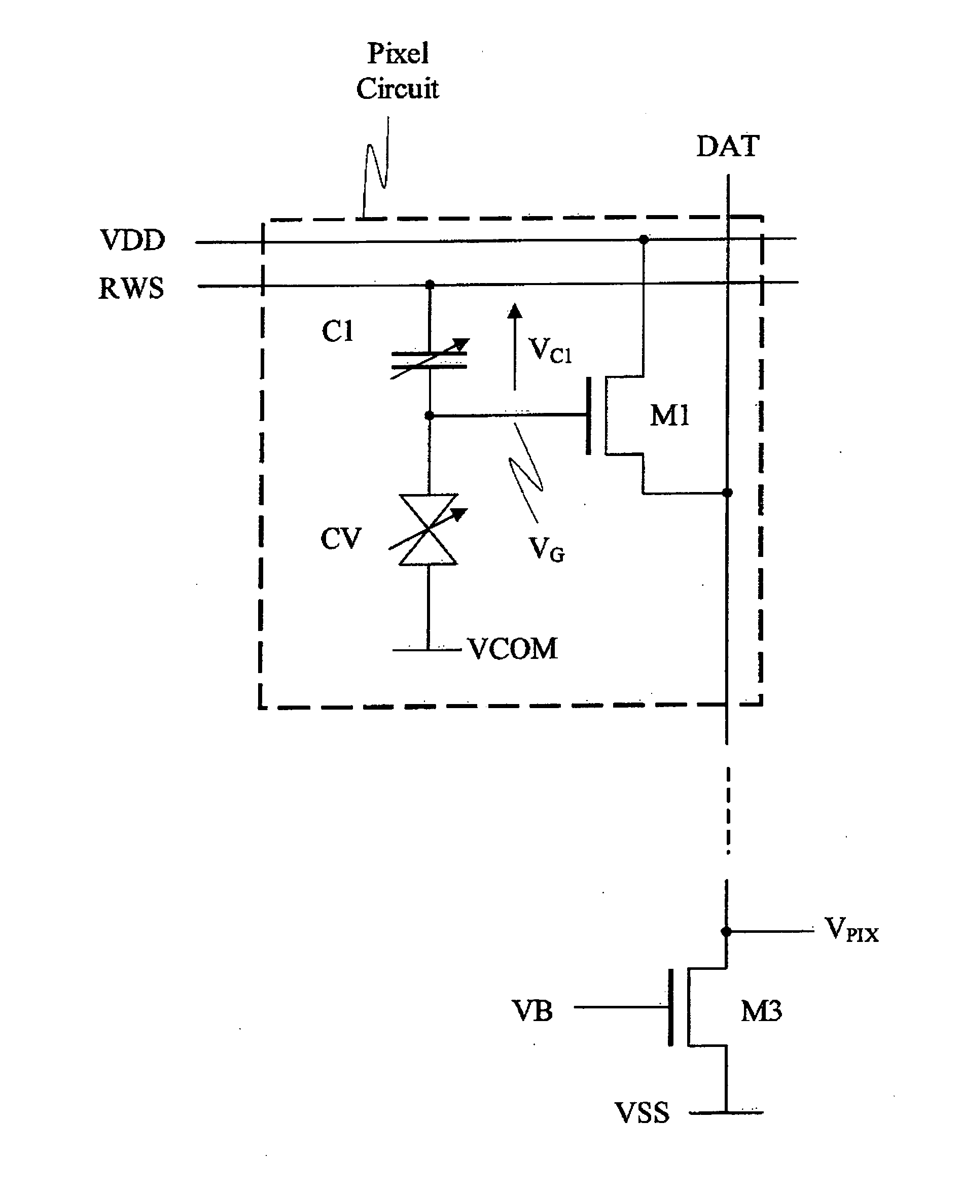
[0095]This embodiment relates to a liquid crystal device comprising an array of sensor circuits. In this embodiment each sensor circuit is an active pixel sensor circuit. As shown in FIG. 9, the active pixel sensor circuit forming a sensor circuit of this embodiment comprises a data line, DAT; a power supply line, VDD; a row select line, RWS; an amplifier, M1; a variable liquid crystal capacitor element, CV which functions in use as a liquid crystal sensing capacitor; and a voltage dependent select capacitor, C1. An input of the amplifier is connected to a terminal of the sensing capacitor.

[0096]Another terminal of the sensing capacitor of each sensor circuit may be connected to common voltage line VCOM such that the another terminal of the sensing capacitors of ...

second embodiment

[0112]In the second embodiment of this invention, the select capacitor of the first embodiment may be formed by a metal-oxide-semiconductor field effect transistor (MOSFET), such as a thin-film transistor (TFT). The transistor may be a p-type transistor with the gate terminal connected to the row select line RWS and the source and drain terminal connected together to the gate terminal of the amplifier transistor. This arrangement is shown in FIG. 14 where the transistor M2 forms the voltage-dependent select capacitor.

[0113]In a first state, where the voltage between the gate and source terminals of the transistor M2, VGS, is less than the threshold voltage of the transistor, VT,M2, the transistor is turned on and exhibits a capacitance, C1A, equal to the sum of the gate-drain, gate-source and gate-channel capacitances (CGD,M2, CGS,M2 and CGC,M2 respectively). In a second state, where the voltage between the gate and source terminals of the transistor M2, VGS, is greater than the thr...

third embodiment

[0115]In the third embodiment of this invention, the select capacitor of the first embodiment may be formed by an n-type transistor. In this circuit, shown in FIG. 15, the gate terminal of the transistor M2 forming the select capacitor is connected to the gate terminal of the amplifier transistor M1 and the source and drain terminals of M2 connected together to the row select line RWS. Again, the transistor exhibits the required voltage-capacitance relationship shown in FIG. 10.

[0116]The operation of this circuit is as described previously for the first and second embodiments.


PUM


Abstract

A liquid crystal device is provided, for example in the form of a combined display and sensor forming a touch screen. The device comprises an array, for example of active matrix type, of sensor circuits. Each sensor circuit comprises a liquid crystal sensing capacitor (CV) connected between a transistor M1 arranged as a source-follower and a precharging input (PRE). A sensor selecting capacitor (C1) is connected between the transistor (M1) and a row select line (RWS).

Description

TECHNICAL FIELD[0001]The present invention relates to liquid crystal devices, for example for use in the field of active matrix liquid crystal displays (AMLCD) with integrated sensors. Such devices may be used for sensing a change in capacitance of a liquid crystal material upon mechanical deformation of the display for creating a touch panel function based on this measurement. Such a touch panel provides information not only about the location of a touch input event but also of the force of touch which is related, via the mechanical deformation, to the magnitude of the change in capacitance.BACKGROUND ART[0002]Circuits to measure the liquid crystal capacitance may be fabricated in a thin-film polysilicon process compatible with that used in the manufacture of the TFT substrate of the AMLCD. In such a system, the pixel matrix must include both sensor and display elements and the same liquid crystal cell used for the display generates the sensor signal. Whilst it is desirable on the ...

Claims


Application Information

Patent Timeline
Patent Type & Authority Applications(United States)
IPC IPC(8): G06F3/044G09G3/36
CPCG06F3/044G06F3/0412G06F3/0446G06F3/0447G06F3/0416
Inventor BROWN, CHRISTOPHER JAMES
Owner SHARP KK
Why Eureka
Try Eureka